Blog
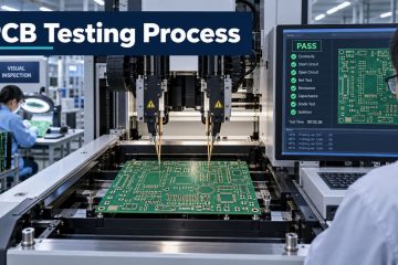
PCB Testing Process: Inspection, Electrical Tests and Release Checks
Understand the PCB testing process from in-process inspection and bare-board electrical testing to reliability qualification, release evidence and supplier checks.



Understand the PCB testing process from in-process inspection and bare-board electrical testing to reliability qualification, release evidence and supplier checks.
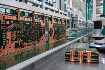
Learn how heavy copper PCB plating builds surface and hole copper, controls current distribution, and verifies thickness, adhesion and microsections before release.
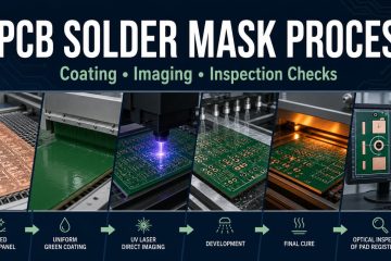
See how PCB solder mask is prepared, coated, imaged, developed, cured and inspected for registration, coverage and adhesion defects.
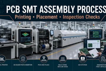
Follow PCB SMT assembly from file and material control through paste printing, SPI, placement, reflow, AOI, X-ray and electrical test.
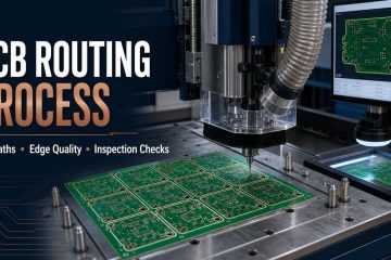
See how PCB CNC routing controls profile data, toolpaths, fixtures, tabs, edge quality, depaneling and dimensional inspection.
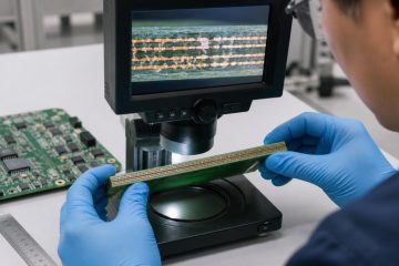
Learn how to identify PCB copper layers using design files, board-edge clues, vias, X-ray, and cross-section evidence, with clear limits for each method.
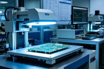
PCB testing is the process of checking a printed circuit board for electrical defects, manufacturing errors, assembly problems and reliability risks before it is used in a final product. A board can look clean from the outside and still have hidden issues such as open circuits, short circuits, poor solder Read more
If you have any enquiry about quotation or cooperation, please feel free to email us at [email protected] or use the following enquiry form. Oursales representative will contact you within 24 hours. Thank you for your interest in our products.