




High-frequency PCB assembly mounts and solders RF, microwave and supporting components while preserving the impedance, loss, grounding and mechanical interfaces designed into the bare board. The line may use familiar SMT equipment, but generic settings are not enough: paste volume, component offset, reflow exposure, residue, connector geometry and housing contact can all become part of the RF signal path.
PCBTRY supports DFM, PCB fabrication, component sourcing, assembly, inspection and customer-defined testing. Send Gerber/ODB++ data, BOM, centroid/CPL, assembly drawings, stackup, approved substitutions, RF connector notes, reflow limits and test specifications for an engineering review and quotation.
What Is the High Frequency PCB Assembly Process?
It is the controlled conversion of a tested RF bare board into an assembled module. The process must protect both ordinary solder-joint reliability and frequency-domain performance. A joint can look acceptable yet change a launch geometry; a connector can pass continuity yet fail return-loss requirements.
How Does the High Frequency PCB Assembly Process Work?
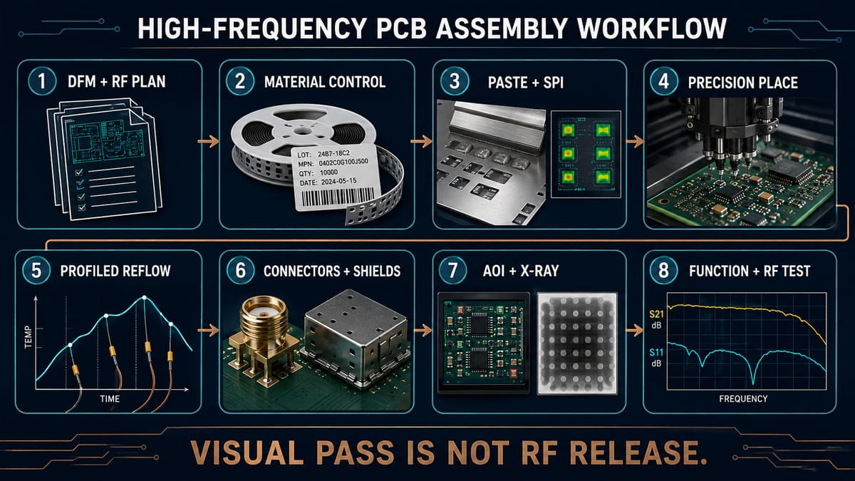
1. Engineering review and assembly DFM. The team aligns PCB revision, BOM, CPL, drawings, RF critical nets, package notes, connector launches, shielding, test points and acceptance limits. Missing side/orientation data can cause placement errors; undefined RF tests can leave a visually good board without a meaningful release criterion.
2. Incoming board and component control. Bare boards are checked against revision, finish, flatness and supplied electrical records. Components are verified by MPN, package, polarity, moisture handling and storage condition. A wrong dielectric lot or passive variant may shift performance even when assembly is defect-free.
3. Solder paste printing and SPI. The stencil deposits paste according to package and process requirements. Paste height, area, position and aperture release are checked where SPI is specified. Excess paste can float small RF passives or alter connector geometry; insufficient paste can create opens or weak ground attachment.
4. Placement and first-article verification. Pick-and-place equipment mounts parts with controlled orientation and offset. Fiducials, package body, terminations and critical launches are inspected. Placement offset matters most where pad and joint geometry contribute parasitics or where shields and housings set mechanical alignment.
5. Profiled reflow soldering. A measured thermal profile is developed for the board mass, laminate, paste and component limits. Thermocouples verify actual locations rather than relying only on oven settings. Too little heat produces incomplete wetting; excessive exposure can damage components, warp the board or stress laminate interfaces.
6. Through-hole, connector, shield and mechanical assembly. Selective, hand or other approved processes attach parts not suited to the main reflow. RF connectors need controlled position, ground attachment and mechanical support; specified fastener sequence and torque belong in the work instruction. Excess solder or misalignment can change the launch.
7. Cleaning and inspection. Flux strategy follows paste, component and customer requirements. If cleaning is required, the method must be compatible with materials and trapped-volume geometry. AOI finds visible polarity, offset and solder defects; X-ray is used for hidden joints when required. Neither test proves RF performance.
8. Electrical, functional and RF release. Continuity, programming, ICT/flying probe, functional checks and RF measurements are selected by product risk. VNA, power, spectrum or system tests require defined fixtures, calibration planes and limits. Compare failures with bare-board or golden-unit evidence to separate assembly defects from design/material issues.
Which Materials and Components Need Special Assembly Control?
| Item | Assembly concern | Release evidence |
| RF laminate/hybrid PCB | Thermal mass, moisture, warpage and finish | Board revision, stackup and incoming record |
| RF passives and filters | Paste volume, orientation and placement parasitics | Package guide, SPI/AOI and RF test |
| QFN/LGA/BGA devices | Thermal-pad paste, hidden joints and voiding | Stencil review, profile and X-ray when specified |
| End-launch/coax connector | Launch alignment, ground solder and mechanical strain | Visual/mechanical check and calibrated RF test |
| Shield can/housing | Coplanarity, soldering sequence and grounding | Work instruction and functional/RF verification |
How Should Reflow Be Profiled for an RF Assembly?
Use the solder-paste supplier’s process window and the most restrictive component/board requirements, then measure the actual assembly. Do not copy peak temperature, ramp or dwell from an unrelated application note. Place thermocouples at thermally light and heavy locations, critical RF packages and areas shielded by metal mass.
The approved profile should identify the assembly revision, load, oven recipe and measured traces. A machine setting is not equivalent to a board temperature record.
What Are the Main High-Frequency Assembly Failure Modes?
| Symptom | Possible assembly cause | Next evidence |
| Continuity passes but return loss worsens | Connector launch, joint geometry, grounding or component shift | Microscope/X-ray as applicable and calibrated VNA comparison |
| Frequency response shifts between units | Wrong passive variant, paste/placement variation or fixture repeatability | Lot trace, SPI/AOI data and fixture repeatability study |
| Intermittent RF output | Weak hidden joint, connector strain or incomplete ground solder | X-ray, mechanical inspection and controlled retest |
| Blister after reflow | Moisture, laminate condition or excessive thermal exposure | Incoming/storage record and measured profile |
| Good board fails only in housing | Connector alignment, grounding, fastener sequence or enclosure coupling | Mechanical datum and torque-controlled A/B test |
How Does Design Affect RF Assembly Reliability?
Design defines whether the process has margin. Correct land patterns, solder-mask strategy, accessible fiducials, balanced thermal mass, supported connectors, rework clearance and test launches make variation observable and controllable. Large ground pads and metal housings can demand more heat than nearby small parts tolerate.
Release the exact package manufacturer guidance and flag RF-critical parts in the assembly drawing. A generic note such as “assemble per standard process” cannot communicate launch geometry or customer-specific RF acceptance.
Which Tests Should Be Used After Assembly?
| Test | Finds | Does not prove alone |
| AOI | Visible placement, polarity and solder anomalies | Hidden joints or RF performance |
| X-ray | Hidden solder structure and gross voiding | Calibrated frequency response |
| ICT/flying probe | Connectivity and component-level faults | System behavior at operating frequency |
| Functional test | Defined powered functions | Full RF specification unless instrumented for it |
| VNA/RF test | Specified S-parameters or RF response | Meaningful results without calibration and fixture control |
What Should a First-Article RF Assembly Review Include?
- Approved BOM, substitutes, PCB and assembly revisions.
- Stencil/aperture exceptions and first-print evidence.
- Critical placement and connector alignment images.
- Measured reflow profile tied to the loaded assembly.
- AOI/X-ray records required by package risk.
- Cleaning or no-clean decision and handling record.
- Mechanical fastening/torque instruction where applicable.
- Fixture, calibration plane, limits and RF test result.
How Long Does High Frequency PCB Assembly Take?
Lead time depends on component availability, bare-board release, stencil and fixture preparation, profile development, first-article review and test capacity. Specialized RF components and custom fixtures can dominate the schedule. Ask the supplier to separate material, engineering, assembly and validation time instead of quoting one unexplained date.
How Do You Choose a High Frequency PCB Assembly Supplier?
Choose a supplier that can connect process evidence to the RF requirement. Ask how revisions and substitutions are controlled, how thermal profiles are measured, which joints require X-ray, how connectors are aligned, and how RF fixtures are calibrated and maintained.
- Can the supplier review PCB fabrication and assembly together?
- Will it document paste, placement and profile decisions for critical parts?
- Can it separate visual, structural, functional and RF acceptance?
- How are rework and post-rework RF retest controlled?
- Which files and limits are required before a firm quotation?
Frequently Asked Questions
Is high-frequency PCB assembly different from normal SMT?
The basic line may be similar, but RF-critical paste, placement, grounding, connectors, cleaning and calibrated tests need added controls.
Can a standard reflow profile be used?
Use a profile developed from the actual board, paste and component limits. Supplier examples are starting information, not an approved recipe.
Does AOI confirm RF performance?
No. AOI verifies visible assembly features; frequency-domain performance requires a defined RF or system test.
When is X-ray required?
Use it when hidden-joint risk or the acceptance plan justifies it, such as BGA/LGA/thermal-pad structures. The customer and assembler should agree the scope and criteria.
Should flux be cleaned from an RF board?
The answer depends on flux chemistry, component restrictions, product environment and customer cleanliness requirements. Follow approved material guidance rather than a universal rule.
Why can an RF connector pass continuity but fail RF test?
Continuity does not measure launch impedance, ground geometry, alignment or mechanical contact. Inspect the launch and test with a calibrated fixture.
What files are needed for quotation?
Send Gerbers/ODB++, BOM, CPL, assembly drawings, stackup, test plan, connector/housing notes, quantities and approved substitution policy.
Should reworked RF boards be retested?
Yes when the rework affects an RF path, reference ground, connector or thermally sensitive region. Define the retest in the repair instruction.
Request an RF PCB Assembly Review
Submit your fabrication data, BOM, CPL, drawings, stackup, critical package guidance and RF acceptance plan to PCBTRY. Engineering review can identify paste, thermal, connector, inspection and fixture gaps before the first article and quotation.



0 Comments