





The PCB testing process verifies whether a finished bare board matches the approved design data and fabrication requirements before components are assembled. It combines in-process inspection, dimensional and structural checks, continuity and isolation testing, final visual acceptance, and any project-specific tests such as controlled impedance or thermal qualification.
No single inspection proves everything. A board can pass an open/short test while still having unacceptable dimensions, damaged solder mask, weak plating, or the wrong material. For an engineering review, send the Gerber or ODB++ package, drill files, fabrication drawing, stack-up, netlist source, impedance table, material notes, acceptance class, and special test requirements to the PCBtry engineering team.
What Is the PCB Testing Process?
The PCB testing process is the controlled comparison of the manufactured board against approved electrical, mechanical, material, and workmanship requirements. It starts before final profiling and continues through shipment release. Bare-board testing is different from PCBA testing: AOI, ICT, X-ray, and functional tests used after component assembly answer different questions.
How Does the PCB Testing Process Work?
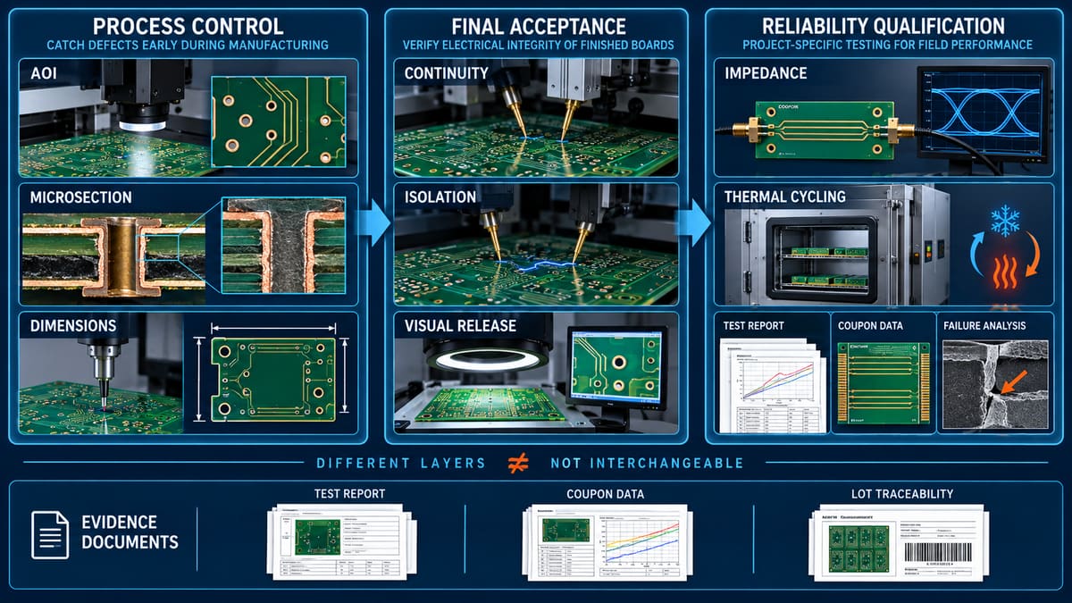
A useful process follows the board’s risk path. Each stage should have an input, an acceptance rule, a recorded result, and a response when the result fails.
1. Confirm the released data and test basis. Engineering locks the board revision, layer data, drill data, drawing, stack-up, netlist source, and special notes. This matters because testing the wrong revision can produce a clean report for the wrong product. The fabrication netlist and customer-supplied design netlist should be compared through a controlled method rather than accepting an unverified file generated from altered production data.
2. Inspect copper patterns during fabrication. Automated optical inspection compares imaged or etched circuitry with reference data and flags opens, shorts, nicks, protrusions, spacing problems, and pattern deviations. AOI catches visible geometry defects early, but it does not by itself prove final plated-hole integrity or all electrical behavior.
3. Verify holes, plating, and internal structure. Dimensional tools check finished holes, slots, outline, thickness, and feature position. Coupons or representative samples may be microsectioned to assess plated-hole structure, layer registration, and material interfaces. A microsection destroys the sample, so the sampling plan and coupon relationship to production panels must be documented.
4. Inspect solder mask, finish, markings, and profile. Inspectors look for exposed or covered pads, mask registration, contamination, finish defects, edge damage, legible markings, bow and twist, and conformity to the drawing. Electrical test cannot detect many of these defects.
5. Run continuity and isolation tests. A flying-probe system or dedicated fixture contacts test points to verify that intended nets conduct and separate nets do not short. The program must match the released netlist, and the test conditions and thresholds must match the procurement specification.
6. Perform specified performance or reliability checks. Controlled-impedance coupons, thermal stress, ionic cleanliness, insulation resistance, solderability, or other tests are included only when required by the design, application, governing specification, or qualification plan. These are not interchangeable with routine open/short testing.
7. Review failures and authorize shipment. Failed boards are segregated and tied to a defect code, disposition, rework or scrap decision, and retest record. Final release checks quantity, revision, test status, traceability, packaging, and requested reports. A pass label without linked records is weak evidence.
Which PCB Test Methods Detect Which Defects?
| Method | What it can reveal | What it does not prove alone |
|---|---|---|
| AOI | Pattern deviations, visible opens/shorts, nicks, spacing and registration issues | Final electrical connectivity, hidden plating quality, material identity |
| Dimensional inspection | Outline, hole, slot, thickness and feature-position conformance | Electrical integrity or internal interfaces |
| Microsection | Representative internal registration, plating and laminate structure | Every board in the lot; it is a destructive sample |
| Flying probe | Continuity and isolation without a dedicated fixture | All visual, dimensional or long-term reliability defects |
| Dedicated fixture | Fast repeatable net testing for suitable production volumes | Correct program/revision unless data control is verified |
| Impedance coupon test | Whether specified coupon structures meet the stated impedance requirement | Every signal path unless coupon correlation and stack-up control are valid |
| Final visual inspection | Finish, mask, legend, edge, cleanliness and handling defects | Hidden electrical or structural defects |
Flying Probe vs. Fixture Testing: Which Should You Choose?
Flying probe is flexible and avoids dedicated fixture construction, which makes it useful for prototypes, engineering changes, and lower quantities. A dedicated fixture contacts many points together and can reduce test time at stable production volume, but it adds tooling, program control, maintenance, and change-management work.
| Decision factor | Flying probe | Dedicated fixture |
|---|---|---|
| Design changes | Program is easier to update | Fixture may require modification |
| Upfront tooling | Usually lower | Fixture design and build required |
| Test throughput | Sequential probing takes longer | Better fit for repeated high-volume tests |
| Access dependency | Still needs reachable features and stable probing | Needs a controlled contact pattern and tooling datums |
| Best question for supplier | What data and thresholds create the program? | How is fixture revision, wear, and maintenance controlled? |
Do not choose only by quantity. Fine-pitch access, board size, repeat orders, revision frequency, required fault coverage, and the cost of an escape all change the decision.
What Does Electrical Testing Prove?
Electrical testing proves that the probed network meets specified continuity and isolation conditions at the time of test. It is effective at finding unintended opens and shorts, but it does not certify laminate, copper thickness, finished dimensions, solderability, impedance, or service life unless those characteristics are tested separately.
The test program is only as trustworthy as its source and revision control. The purchase package should identify the electrical test requirement, any excluded nets or non-tested features, and the expected report or certificate.
How Are Plated Holes and Internal Layers Checked?
Plated holes and internal layers require a combination of process records, AOI, dimensional measurement, representative coupon evaluation, and—when specified—microsection or stress testing. The inspection plan should connect the sample or coupon to its production panel and lot.
A polished cross-section can reveal layer registration, hole-wall structure, resin condition, and plating anomalies at that location. It is strong evidence for the inspected sample, not proof that every feature on every board is identical. Buyers should ask how sampling, coupon placement, and escalation after a failure are defined.
When Is Controlled-Impedance Testing Needed?
Controlled-impedance testing is needed when the drawing or stack-up specifies impedance requirements for high-speed, RF, differential, or other controlled transmission lines. The manufacturer normally builds representative test coupons with the panel and measures them using an appropriate method.
Provide target impedance, tolerance, layer, trace type, reference plane, stack-up, material constraints, and coupon/report requirements. A generic “impedance control” note without structures and acceptance limits leaves the factory to guess.
How Do Acceptance Tests Differ from Reliability Tests?
Acceptance tests decide whether a board or lot conforms now; reliability tests challenge samples to evaluate how the design and process behave under expected stress. Passing one does not replace the other.
| Test layer | Decision | Typical evidence |
|---|---|---|
| In-process control | Can production continue? | AOI results, process measurements, coupon records |
| Final acceptance | Can this board or lot ship? | Electrical-test status, dimensional/visual records, release inspection |
| Reliability qualification | Is the design/process suitable for stated stress? | Test plan, sample identity, stress history, measurements, failure analysis |
Environmental and life tests must come from the product’s actual risk and applicable requirements. Copying an unrelated chamber cycle creates data without a useful decision.
What Common PCB Testing Failures Matter?
- Open circuit: an intended connection is interrupted by etching, crack, poor plating, or damage.
- Short circuit: copper or conductive contamination joins nets that should remain isolated.
- Annular ring or registration problem: drilling and layer alignment reduce the intended copper capture.
- Plating anomaly: the hole wall or surface deposit has a structural or thickness-related defect that requires specified inspection.
- Mask or finish nonconformance: pads are incorrectly exposed/covered, contaminated, damaged, or unsuitable for the next operation.
- Impedance deviation: the manufactured stack-up and geometry do not produce the specified coupon result.
- Revision escape: the physical board or test program does not match the approved release.
What Test Evidence Should a Buyer Request?
Request evidence that matches project risk instead of asking for “all reports.” The useful package identifies the board revision, lot, test basis, result, exceptions, and authorization.
- Electrical-test confirmation and method
- Netlist/test-data revision and any exclusions
- Controlled-impedance coupon results when specified
- Microsection or coupon report when contractually required
- Material and surface-finish documentation required by the purchase order
- Dimensional or special-characteristic results where critical
- Nonconformance, repair, concession, and retest status
- Lot and panel traceability tied to shipment quantity
How Should You Choose a PCB Testing Supplier?
Choose a supplier that can explain the defect coverage and limitation of each inspection, control data revisions, show how failed boards are segregated and retested, and provide evidence tied to the shipped lot. Equipment lists alone do not prove the process is controlled.
Ask who approves the test program, how changes are verified, which characteristics are 100% tested versus sampled, how fixture wear is monitored, and what triggers root-cause analysis. Confirm that the supplier can support the required stack-up and PCB testing scope before placing the order.
Frequently Asked Questions
Is every bare PCB electrically tested?
Do not assume the coverage or method. State the electrical-test requirement in the purchase data and ask the manufacturer to confirm whether every board, a panel, or a defined sample is tested.
Does a flying-probe test check components?
For a bare PCB, it checks unpopulated electrical networks. Flying-probe systems can also be configured for some assembled-board work, but that is a different program and coverage plan.
Can AOI replace electrical testing?
No. AOI evaluates visible geometry against reference data, while electrical testing measures continuity and isolation at accessible points. The methods find overlapping but different defect classes.
What standard applies to bare PCB visual acceptance?
IPC-A-600 is widely used for printed-board acceptability, together with the applicable performance specification, fabrication drawing, purchase requirements, and agreed revision. IPC-A-610 addresses electronic assemblies and should not be substituted as the primary bare-board acceptance document.
What files are needed to create the electrical test?
Provide the controlled fabrication data and an authoritative design netlist or approved intelligent data package, plus drill files, drawing, stack-up and special test notes. Agree how the manufacturer validates the test program against the released design.
Does passing electrical test guarantee reliability?
No. It confirms specified electrical conditions at test time. Reliability depends on structure, materials, process stability, environment, assembly, and application-specific qualification.
How are repaired boards handled?
The purchase agreement should define permitted repairs, approval authority, traceability, inspection, and complete retest after repair. Safety- or reliability-critical projects may prohibit certain repairs.
Should prototypes and production use the same test method?
Not necessarily. Flying probe may fit changing prototypes while a fixture may fit stable volume, but the required fault coverage and acceptance criteria should remain controlled through the transition.
Build the Test Plan Before Fabrication Starts
The best time to define testing is during design and RFQ review, not after finished boards reach final inspection. Send PCBtry your Gerber or ODB++ data, drill files, stack-up, drawing, netlist, impedance requirements, application risks, acceptance criteria, and requested reports for a manufacturing and test review before quotation.



0 Comments