





The PCB reflow process heats a printed solder-paste deposit and placed surface-mount components through a controlled thermal cycle so the alloy melts, wets the terminations and pads, and cools into stable solder joints. Reliable reflow depends on the stencil, paste, components, PCB design, moisture control, measured thermal profile, oven loading, atmosphere, cooling, and inspection working as one system.
A copied oven recipe is not a qualified process. Before production, provide the BOM, approved substitutions, paste/alloy requirements, component temperature limits, MSL handling, PCB finish, stack-up, panel drawing and acceptance/test plan. PCBtry can review these inputs as part of PCB assembly engineering before quotation.
What Is the PCB Reflow Process?
PCB reflow is the SMT soldering stage that turns accurately printed paste and placed components into permanent electrical and mechanical joints. The oven creates the heat environment, but thermocouples on a representative assembly show what critical solder joints, packages and board regions actually experience.
How Does the PCB Reflow Process Work?
The process starts before the board enters the oven and ends only after inspection data has been reviewed.
1. Confirm materials and thermal limits. Engineering verifies the solder paste, alloy, flux system, PCB finish, component ratings, moisture sensitivity, panel construction and acceptance requirements. A profile must fit the paste supplier’s recommended window without exceeding the limits of sensitive components or the PCB.
2. Prepare paste, stencil and PCB. Paste storage, conditioning, mixing and working time follow the approved material instructions. Stencil thickness, apertures, cleanliness, board support and printer setup control deposit volume and symmetry. Reflow cannot consistently repair a poor print.
3. Print, inspect and place components. Solder paste inspection checks height, area, volume, offset and bridging risks before placement. Placement then controls polarity, rotation, position and seating. Excess paste, an offset part or unequal deposits can become a bridge or tombstone in the oven.
4. Instrument a representative assembly. Thermocouples are attached to thermally demanding and sensitive locations, including large thermal masses, small passives, hidden joints and different board regions. The profiled panel, fixture and loading condition should represent production.
5. Run preheat and thermal equalization. The assembly warms at a controlled rate. Flux activates, volatiles begin to escape and temperature differences across the assembly are reduced. Heating too aggressively can promote splatter, warpage or component stress; excessive exposure can exhaust flux before wetting.
6. Reach liquidus and peak. Solder becomes molten and must remain in the effective reflow window long enough to wet without overexposing components, laminate or flux. The required limits come from the approved paste, alloy, component and product requirements—not a generic web recipe.
7. Cool under control. Joints solidify while components and the PCB contract. Cooling affects joint formation and thermal stress; movement before solidification can disturb the joint.
8. Inspect, classify and improve. AOI checks visible placement and solder features; X-ray evaluates hidden joints when required; electrical or functional tests address behavior. Engineers connect defects back to SPI, placement, profile, design, materials and handling before changing the oven.
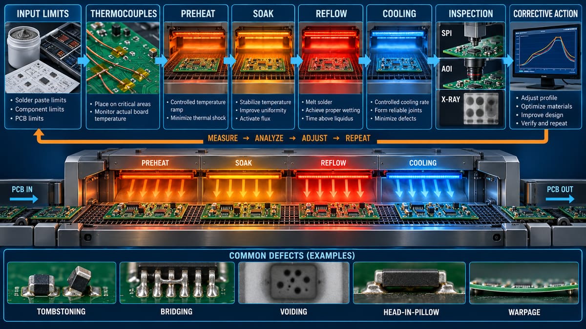
What Does Each Reflow Zone Need to Achieve?
| Stage | Required outcome | Risk when control is poor |
|---|---|---|
| Preheat | Controlled assembly warming | Thermal shock, splatter, warpage or excessive temperature difference |
| Soak/equalization | Reduce thermal imbalance and support flux action | Flux exhaustion, oxidation or unequal wetting |
| Reflow | All required joints melt and wet within material limits | Cold/non-wet joints, damage, voiding or head-in-pillow |
| Cooling | Stable solidification without movement or excessive stress | Disturbed joints, board stress or poor joint structure |
How Is a Reflow Profile Measured?
A profile is measured with calibrated thermocouples attached to selected locations on a representative board. The data logger travels through the production oven and records temperature over time. Oven zone settings and conveyor speed are inputs; the thermocouple traces are the product evidence.
Select locations from thermal risk: the largest and smallest masses, corners and center, shielded areas, bottom-terminated parts, heat-sensitive components and known problem joints. Record board revision, panel, paste, oven, line, conveyor setup, loading and attachment method so the result is reproducible.
Why Can One Oven Recipe Produce Different Board Temperatures?
Board copper, planes, thickness, panel utilization, component mass, shielding, pallets, conveyor loading and airflow change heat transfer. A recipe that works for a light board may leave a large connector joint too cold or expose a small nearby component too long.
Use a product family only when evidence shows the thermal constructions are genuinely comparable. Re-profile when a change alters thermal mass, paste/alloy, panel, fixture, oven, airflow, critical components or recurring defect behavior.
What Causes Common Reflow Defects?
| Defect | Possible mechanism | First evidence to review |
|---|---|---|
| Tombstoning | Unequal paste, pad design, heating or placement creates unbalanced wetting | SPI, pad/thermal symmetry, placement and local profile |
| Bridging | Excess or displaced paste, stencil/design issue or component offset | SPI, stencil aperture, placement and solderability |
| Voiding | Volatiles become trapped; pad/paste/design and profile interact | X-ray, paste, pad geometry and measured profile |
| Head-in-pillow | Package/board warpage separates molten surfaces while oxidation limits wetting | X-ray, warpage, paste condition and thermal history |
| Graping/non-wetting | Flux loses effectiveness or surfaces are oxidized/contaminated | Paste exposure, finish/termination, print volume and profile |
| Board warpage | Construction, support and thermal gradients deform the assembly | Panel/fixture, stack-up, measured delta and oven support |
A defect name does not prove a single cause. Change one controlled variable at a time and confirm the effect through inspection data.
How Do PCB Design and Stencil Design Affect Reflow?
Pad geometry, thermal connections, copper imbalance, component spacing, orientation, solder-mask definition, via placement and panel support influence paste release, heating and wetting. Stencil apertures determine how much paste reaches each joint and whether deposits are balanced.
Flag heavy copper regions next to tiny passives, bottom-terminated components, large connectors, mixed finishes and densely shielded areas during DFM. Profile tuning cannot fully compensate for a layout that creates conflicting thermal and paste requirements.
How Are Moisture-Sensitive Components Controlled?
Moisture-sensitive devices require packaging, exposure tracking, storage and any baking to follow the component supplier and applicable handling requirements. Absorbed moisture can expand during reflow and damage a package even when the oven profile is otherwise compliant.
The build record should link component lots, floor-life status, dry storage or baking evidence and reflow time. Baking is not a universal reset; excessive or incorrect baking can affect packaging, terminals or solderability.
Which Inspections Belong Around Reflow?
SPI belongs before placement/reflow because paste variation is an upstream predictor. AOI belongs after soldering for visible defects. X-ray is useful for hidden joints such as BGA and bottom-terminated packages when required. Electrical and functional testing verifies circuit behavior that images alone cannot prove.
The inspection plan should match component technology and risk. AOI cannot see every hidden interface, and an X-ray image does not by itself prove joint metallurgy or full functional performance.
What Evidence Should a Buyer Request?
- Approved paste/alloy and relevant material handling records
- Stencil revision and printer/SPI control tied to the PCB revision
- Measured thermocouple profile with locations and production conditions
- Change and revalidation triggers
- AOI/X-ray/electrical test coverage and acceptance basis
- Defect classification, nonconformance and retest records
- Component moisture-control traceability where applicable
- First-article approval and lot/revision traceability
How Do You Choose a Reflow Assembly Supplier?
Ask how the supplier develops profiles, selects thermocouple points, controls paste and MSL exposure, reviews SPI/AOI/X-ray data, and handles a recurring defect. A long oven does not prove process control.
Confirm the supplier can handle your board’s thermal mass, smallest deposits, largest packages, hidden joints, panel support and inspection requirements. Send the complete manufacturing package rather than only Gerbers.
Frequently Asked Questions
Is reflow temperature the same as the oven setpoint?
No. The setpoint controls each oven zone; the product temperature is measured by thermocouples attached to the assembly.
Can one reflow profile be used for every PCB?
Only when validation shows the boards have compatible materials, thermal mass, components, paste and loading. Otherwise, profile the representative product.
Does a slower conveyor always improve soldering?
No. It changes exposure in every zone and can overheat materials or exhaust flux. Adjust settings against measured product traces and defect evidence.
Can AOI detect BGA head-in-pillow?
AOI cannot directly see hidden BGA interfaces. X-ray and additional analysis may be required depending on geometry and defect type.
Why do small components tombstone?
Unequal wetting forces can lift one end. Review paste volume, placement, pad/thermal symmetry and the local thermal profile together.
When should a board be re-profiled?
Re-profile after changes that affect thermal behavior or when defects show the process is no longer stable. Define triggers before production.
What files are needed for a reflow review?
Provide Gerbers or ODB++, stack-up, panel drawing, BOM, CPL, assembly drawings, stencil notes, paste/alloy requirement, MSL information and acceptance/test criteria.
Does a good profile guarantee reliable solder joints?
No. Printing, materials, design, placement, contamination, warpage and inspection coverage also control the result.
Submit the Assembly Package Before Profiling
For DFM, process planning and quotation, contact PCBtry with the PCB data, BOM, CPL, assembly drawings, paste/alloy and finish requirements, component thermal/MSL constraints, panel information and inspection criteria. The goal is a measurable process window and an evidence-based release plan.



0 Comments