




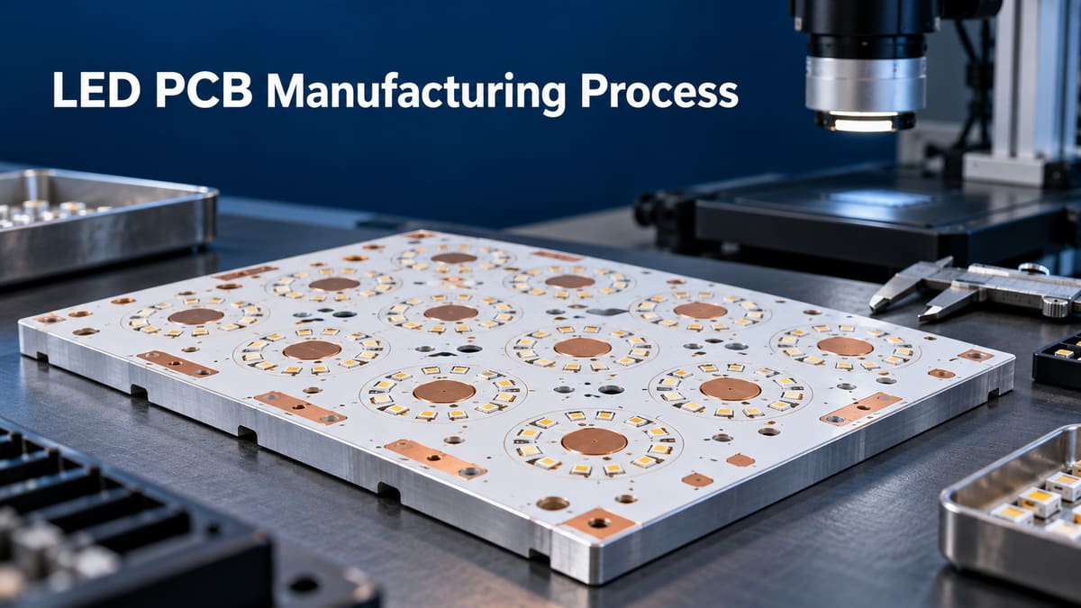
The LED PCB manufacturing process turns circuit data and thermal requirements into a board that routes current, supports the LED package, and moves heat toward a heatsink or enclosure. These boards are used in luminaires, automotive lighting, displays, UV equipment, medical devices, and industrial indicators. Compared with an ordinary low-power control board, an LED board must be released as part of a thermal system: copper, dielectric, vias, metal base, thermal interface material, enclosure, and airflow all affect operating temperature.
pcbtry supports stack-up review, DFM, bare-board fabrication, and assembly/test planning for LED PCB projects. Send Gerber or ODB++ data, drawings, LED and driver information, thermal assumptions, quantities, and acceptance tests for an engineering review and quotation. The goal is to resolve thermal and manufacturing conflicts before tooling rather than discover them after LEDs are assembled.
What Is an LED PCB?
An LED PCB is a printed circuit board designed to mount and interconnect light-emitting diodes and their supporting circuitry. It may be a conventional FR-4 board, an insulated metal substrate (IMS/MCPCB), a copper-base board, or a ceramic circuit. “LED PCB” describes the application; it does not define one material or one factory route.
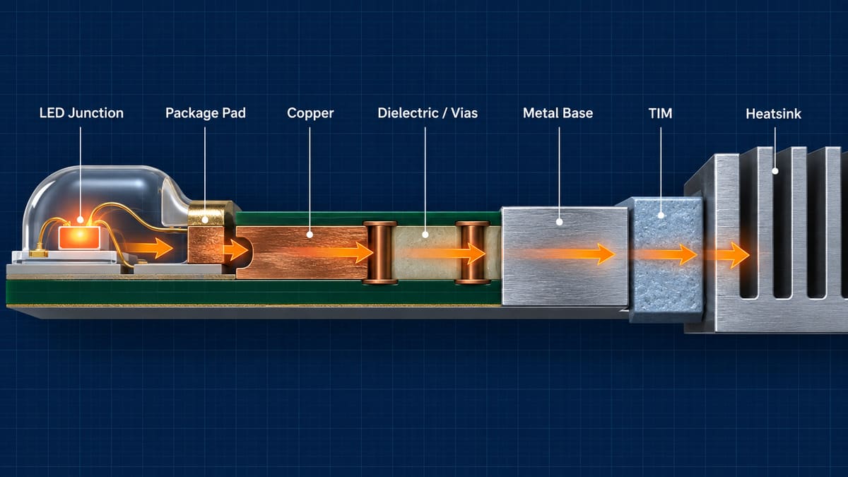
The manufacturing difficulty comes from coupling electrical, optical, thermal, and mechanical interfaces. A board can pass continuity testing yet still run too hot because heat is trapped at the package pad, dielectric, thermal vias, interface material, or heatsink. That is why the release package must define the intended construction and the system boundary used for validation.
How Does the LED PCB Manufacturing Process Work?
The process starts with engineering release and ends with evidence against the drawing. Bare-board fabrication is the core scope; LED placement, reflow, optical checks, and system thermal validation are downstream operations that must be quoted separately when required.
1. Engineering review and DFM analysis. CAM and process engineers reconcile Gerber or ODB++ data, drill files, stack-up, finished thickness, copper, dielectric, board outline, surface finish, solder mask, tolerances, test data, panel requirements, and the intended assembly. They also confirm where heat is generated and where it is expected to leave the board. Missing thermal-pad geometry, conflicting drill data, or an undefined metal-core isolation requirement should become an engineering question; guessing can create an electrically correct but thermally weak build.
2. Stack-up and material release. The team selects an approved construction: FR-4 with thermal vias, aluminum IMS, copper-base IMS, ceramic, or a hybrid/multilayer route. For IMS, the thermal dielectric must provide electrical isolation while transferring heat; for FR-4, copper spreading and the via network become more important. Material identity, thickness, copper construction, flammability or compliance needs, surface condition, and approved alternatives are locked before production. A trade name alone is not enough because different grades can have different thermal and processing behavior.
3. Circuit imaging and copper formation. The conductor pattern is imaged and etched for subtractive constructions, or built by the route specified for the selected substrate. The factory controls artwork scaling, exposure, development, etch condition, conductor width, spacing, and pad shape. Excessive undercut can narrow high-current paths; residue or imaging defects can leave shorts, opens, or reduced isolation. Fine LED pads also need geometry that remains manufacturable after finish and solder mask registration.
4. Lamination or dielectric bonding. Multilayer FR-4 constructions are registered and laminated; IMS constructions bond the copper circuit layer to the metal base through a thermally conductive dielectric system. Temperature, pressure, cleanliness, resin or adhesive flow, material compatibility, and thickness distribution are controlled for the chosen system. Voids, contamination, poor bonding, or excessive flow can degrade dielectric integrity, flatness, registration, and the thermal path.
5. Drilling, thermal vias, and plating. FR-4 LED boards may use plated thermal vias under or near exposed pads; multilayer boards use vias for electrical interconnection; IMS projects may include mechanically drilled holes or specialized structures permitted by the supplier. Hole preparation and copper plating must create a continuous, inspectable connection without breakout, debris, plating voids, or unintended contact to the metal base. A dense via pattern is not automatically better: pitch, finished hole, annular ring, solder wicking, paste design, and assembly method must be reviewed together. For layout guidance, see thermal via design for high-power components.
6. Solder mask, surface finish, legend, and profiling. Solder mask defines exposed LED and component pads, protects conductors, and can influence optical appearance around the light source. The surface finish must suit soldering, storage, and assembly requirements. The board is then routed, scored, punched, or otherwise profiled using a qualified method. Misregistered mask can reduce the solderable pad; poor finish control can affect wetting; burrs, damaged dielectric, or a deformed metal base can prevent proper contact with the heatsink.
7. Bare-board inspection and electrical test. AOI and visual inspection check circuit geometry, mask, finish, markings, and surface condition. Dimensional inspection checks profile, holes, thickness, flatness, and critical interfaces. Electrical testing verifies continuity and isolation against released test data; additional dielectric or microsection evidence is added when specified. Electrical test proves the netlist—not thermal performance, LED polarity, light output, or system life.
8. Optional assembly and application validation. If assembly is included, the process adds paste printing or dispensing, component placement, polarity control, reflow or selective soldering, cleaning where required, AOI/X-ray as applicable, and functional checks. Thermal validation then measures the assembled product under defined power, ambient, mounting, TIM, heatsink, airflow, and stabilization conditions. Optical output and color checks require agreed instruments and limits. These results cannot be inferred from a bare-board certificate.
Which Stack-Up Should You Choose for an LED PCB?
Choose the least complex construction that meets the electrical isolation, temperature, mechanical, routing, reliability, and cost requirements. Do not choose from a generic “thermal conductivity” number alone; interface resistance, thickness, copper coverage, mounting, and the final heatsink can dominate the result.
| Construction | Good fit | Main limitation | Release questions |
|---|---|---|---|
| FR-4 with copper spreading and thermal vias | Lower-to-moderate heat loads, multilayer routing, integrated controls | Heat must cross organic dielectric and via interfaces | Via structure, paste/wicking control, copper balance, board-to-chassis path |
| Aluminum IMS / MCPCB | Single- or limited-layer LED boards needing a direct, economical base-to-heatsink interface | Routing freedom and through-hole structures can be constrained | Dielectric system, isolation, metal thickness, flatness, profiling and mounting |
| Copper-base IMS | Higher heat spreading or mechanically demanding localized loads | Weight, material cost, processing and stress require review | Base grade/thickness, bonding system, copper balance and attachment |
| Ceramic substrate | Compact high-temperature, high-isolation, power or specialized optoelectronic modules | Brittle handling, metallization route, tolerances and cost differ from standard PCB work | Ceramic grade, metallization, finish, edge criteria and assembly interface |
For a deeper metal-core construction overview, review metal-core PCB thermal management. Ask the selected factory to return a controlled stack-up rather than accepting an unqualified material substitution.
How Is Heat Removed from the LED?
Heat moves from the LED junction through the package and soldered thermal pad into copper, then through a dielectric, thermal-via field, metal base, or ceramic substrate. It continues through the board-to-heatsink interface and finally reaches ambient air or coolant. The weakest interface can limit the whole path.
A useful thermal specification therefore identifies power dissipation, duty cycle, ambient range, allowable component or junction target, package thermal-pad construction, board mounting, thermal interface material, heatsink, and airflow. If the LED supplier provides a measurement point or thermal characterization method, use it consistently. Comparing two boards on different heatsinks or before both assemblies reach thermal equilibrium does not isolate PCB performance.
What Manufacturing Challenges Cause LED PCB Failures?
Most failures are not caused by a single dramatic defect. They arise when several acceptable-looking interfaces combine into an inadequate electrical, thermal, or mechanical path.
| Risk | Likely cause | Process control | Buyer evidence |
|---|---|---|---|
| LED runs hot despite electrical pass | Wrong stack-up assumption, dielectric bottleneck, poor TIM contact, insufficient heatsink | Thermal-path review with defined system boundary | Released stack-up and application test conditions |
| Dielectric breakdown to metal base | Damage, contamination, inadequate isolation geometry, route mismatch | Material/edge control and specified dielectric test | Test method, limit, sample scope and results |
| Poor LED solder joint or tilt | Pad/mask/paste imbalance, finish issue, uneven heating | Footprint and stencil review; controlled reflow | AOI/X-ray or first-article evidence as applicable |
| Open or resistive thermal via | Drill debris, plating void, unsuitable via construction | Hole preparation, plating control and section review | Electrical test plus microsection when required |
| Board does not seat on heatsink | Warp, burr, protrusion, wrong mounting tolerance | Profile, flatness and mechanical-interface inspection | Dimensional report and controlled packaging |
| Early lumen/color drift | Excess temperature, drive condition, optical material or assembly stress | System-level thermal and optical validation | Defined power/ambient/measurement plan—not only PCB COC |
How Do Layout and Assembly Affect Reliability?
Layout decides how current and heat spread before the factory begins. Keep the manufacturer’s copper, clearance, via, mask, routing, and panel rules visible during component placement. Place the thermal path beneath or close to the LED package as intended by its datasheet; avoid necking the heat-spreading copper; and review copper balance where large metal areas can affect flatness.
Assembly adds another coupled process. Unequal pad geometry or paste volume can rotate or tilt an LED, while excessive dwell or repeated rework can damage pads, laminate, package, or optical surfaces. Polarity and orientation need unambiguous centroid data, assembly drawings, and first-article inspection. A joint may look shiny yet still have insufficient wetting beneath an exposed thermal pad, so the inspection method must match the hidden interface.
What Tests Verify LED PCB Quality?
Use a layered test plan. Each test should answer one question and have an agreed method, limit, sampling rule, and disposition for failure.
- Material and construction: verify approved material identity, thickness, copper, dielectric system, finish, and traceability.
- Dimensional and visual: check profile, holes, flatness, pad/mask registration, finish, base condition, burrs, and cleanliness.
- AOI and electrical test: find pattern defects and verify continuity/isolation against the released netlist.
- Cross-section or process coupons: evaluate plating, via condition, interfaces, or dielectric construction when the drawing requires it.
- Dielectric verification: use the specified method for insulation to a metal base; do not invent a test voltage at purchase time.
- Assembly inspection: verify polarity, alignment, solder wetting, bridges, void-sensitive hidden pads, and workmanship with the method suited to the package.
- Functional/optical test: define drive current, channels, light output/color criteria, instruments, fixtures, and test duration.
- Thermal validation: define power, ambient, mounting torque, TIM, heatsink, airflow, measurement point, and stabilization condition.
How Long Does LED PCB Manufacturing Take?
There is no honest universal lead time. Schedule depends on material availability, whether the stack-up is already qualified, layer count, thermal-via or metal-base construction, finish, outline method, panel utilization, test documentation, assembly parts, and first-article approval.
Ask the supplier to separate DFM response, material procurement, bare-board fabrication, assembly, validation, and shipping. A prototype with a standard released construction can be quicker than a “simple” board that requires a new dielectric, custom metal thickness, unusual outline, optical bin control, or system thermal fixture.
How Do You Choose an LED PCB Manufacturer?
A reliable manufacturer should turn the application into a controlled construction and explain which evidence proves each critical interface. Compare engineering responses, not just quoted substrate labels.
- Ask which FR-4, IMS, copper-base, and ceramic routes are actually supported.
- Request route-specific design rules and an approved stack-up.
- Confirm how metal-base isolation, flatness, profiling, and thermal vias are controlled.
- Separate bare-board tests from assembly, optical, and system thermal tests.
- Ask which inspections are in-house and which are subcontracted.
- Define material substitution, lot traceability, first-article approval, and nonconformance handling.
- Submit the same drawings and acceptance plan to every bidder before comparing price.
A broader DFM and DFA review is especially useful when the PCB, stencil, placement, enclosure, and heatsink are controlled by different teams.
What Files and Specifications Are Needed for an RFQ?
- Gerber or ODB++ data, NC drill/router files, netlist, and revision identification;
- fabrication drawing, released stack-up, finished thickness, copper, surface finish, mask, profile, tolerances, and panel needs;
- approved laminate, IMS dielectric/metal base, ceramic grade, or permitted equivalents;
- LED and driver datasheets, power/duty assumptions, polarity, and critical thermal-pad information;
- pick-and-place/CPL, BOM with manufacturer part numbers, assembly drawing, stencil notes, and reflow restrictions if assembly is quoted;
- heatsink, TIM, mounting, ambient, airflow, and thermal measurement boundary;
- electrical, dielectric, optical, thermal, workmanship, inspection, documentation, and traceability requirements;
- prototype and production quantities, packaging, delivery destination, and approval stages.
Frequently Asked Questions
Is every LED PCB an aluminum PCB?
No. Aluminum IMS is common, but FR-4 with thermal vias, copper-base IMS, ceramic, and multilayer constructions can be appropriate. Power density, routing, isolation, mechanics, cost, and the final heatsink determine the route.
What is the difference between an LED PCB and an LED PCB assembly?
The PCB is the fabricated bare board. The assembly adds LEDs, drivers, connectors, solder joints, polarity control, and functional checks; system thermal and optical validation may still be a separate scope.
Can an electrical test prove that the LED board will run cool?
No. Continuity and isolation testing confirm the netlist. Thermal performance depends on the assembled LED, board construction, interface material, mounting, heatsink, airflow, power, and ambient conditions.
Are more thermal vias always better?
No. Via size, pitch, plating, solder wicking, pad geometry, paste design, copper planes, and the destination of the heat all matter. The pattern should be reviewed as part of the package and assembly process.
Which surface finish is best for LED PCBs?
There is no universal answer. Choose a finish compatible with the soldering process, component pitch, storage, reliability, wire bonding if applicable, and the manufacturer’s controlled capability.
Why does an LED tilt during reflow?
Unequal pad geometry, solder mask definition, paste volume, wetting, component placement, or heating can create unbalanced surface-tension forces. Review the footprint, stencil, finish, placement, and reflow evidence together.
What should a thermal test report include?
It should identify the sample, power and duty cycle, ambient, airflow, TIM, heatsink, mounting method, measurement location/instrument, stabilization criterion, and result. Without those conditions, results from two tests are not directly comparable.
What causes two LED PCB quotations to differ?
Suppliers may assume different materials, dielectric systems, metal thicknesses, tolerances, finishes, panel yields, tests, documentation, or assembly scope. Normalize the released construction and acceptance plan before comparing unit price.
Request an LED PCB Engineering Review
An actionable quote should confirm the stack-up, heat-path assumptions, manufacturing route, test boundary, and unresolved risks. Send your PCB files, drawings, LED/BOM data, thermal and mechanical conditions, quantities, and acceptance requirements to [email protected]. pcbtry can then review the construction before tooling and quote the required bare-board, assembly, inspection, and validation scope.



0 Comments