Industrial PCB Manufacturing Process: Controls, Testing and Supplier Checks
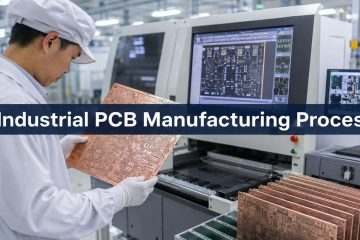
Follow the industrial PCB manufacturing process from DFM and material control through imaging, lamination, plating, finishing, inspection, testing and supplier release.
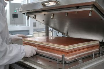
Learn how high-frequency multilayer PCBs are laminated, including material compatibility, surface preparation, registration, press control and post-lamination RF checks.
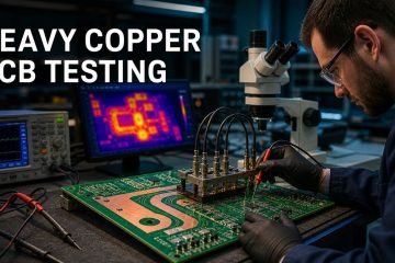
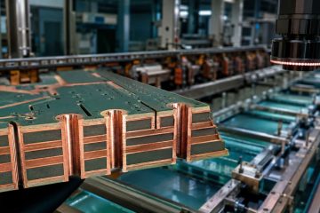
See how heavy copper PCBs move from DFM and stack-up review through plating, etching, lamination, drilling and release testing—with buyer checks at each stage.
Learn how heavy copper PCBs are checked for copper geometry, plated-hole integrity, resistance, current capacity, temperature rise and reliability.
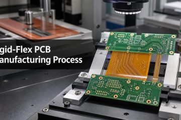
See how rigid-flex PCBs are built, which process controls prevent transition and plating failures, and what test evidence to request before ordering.
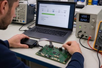
Learn how to identify a PCB programming interface, match firmware to the target, connect safely, flash the device, diagnose failures and verify the result.
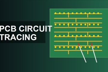
Learn how to trace a PCB circuit by following visible tracks, using continuity mode correctly, marking nets, checking components and preparing repair or remake notes.
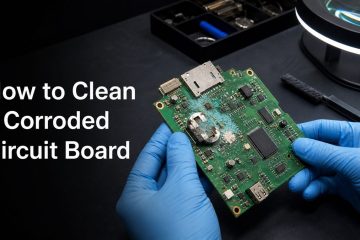
Learn how to identify the residue, clean a corroded circuit board safely, inspect damaged traces and pads, and test it before controlled power-up.
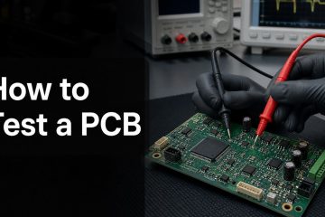
Learn how to test a PCB safely with visual inspection, multimeter checks, controlled power-up, fault isolation and clear pass/fail evidence.
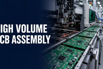
Plan a safer high volume PCB assembly ramp with readiness gates, test coverage, traceability, cost drivers, supplier questions, and an RFQ checklist.
If you have any enquiry about quotation or cooperation, please feel free to email us at [email protected] or use the following enquiry form. Oursales representative will contact you within 24 hours. Thank you for your interest in our products.