




The industrial PCB manufacturing process turns controlled design data into bare circuit boards that can survive the electrical, thermal, mechanical and service conditions of industrial equipment. The fabrication sequence resembles other multilayer PCB production, but industrial projects need tighter revision discipline, material traceability, defined acceptance evidence and a clear response when a process or supplier changes.
The useful question is not whether a factory owns drilling, plating and test equipment. It is whether the supplier can connect your design requirements to controlled production records and release evidence. PCBtry supports fabrication review and production planning; send Gerber files, NC drill data, stackup, fabrication drawing, quantity and acceptance requirements through the contact page for an engineering review and quotation.

What Makes an Industrial PCB Manufacturing Process Different?
An industrial PCB is manufactured for equipment such as automation controllers, drives, power converters, instrumentation and infrastructure electronics, where long service life and difficult environments can make a small fabrication variation expensive. “Industrial” is not a single laminate or acceptance class. The application defines the needed material system, copper structure, spacing, coating compatibility, testing and documentation.
A buyer should therefore translate field conditions into build requirements. Temperature cycling affects resin and plated connections. Moisture and contamination influence surface insulation. Vibration can expose weak mechanical support. High current raises copper and thermal concerns. The fabrication drawing and purchase specification must state the requirements that the factory is expected to control.
Which Inputs Must Be Reviewed Before Production Starts?
Production should start from one approved data package with no conflicting revisions. At minimum, provide Gerber or other accepted image data, NC drill files, a controlled stackup, board outline, fabrication drawing, material requirements, copper weights, surface finish, impedance notes where applicable, panel or delivery requirements, quantity and acceptance criteria.
| Input | Engineering check | Risk if unclear |
| Gerber and drill data | Layer names, polarity, drill pairing and revision | Wrong layer or hole structure |
| Stackup | Dielectric system, copper distribution and finished thickness | Impedance, bow/twist or lamination mismatch |
| Fabrication drawing | Dimensions, tolerances, finish, markings and special notes | Supplier assumptions become acceptance disputes |
| Acceptance plan | Inspection, test, coupon and report requirements | A passing shipment may not prove application fitness |
A formal DFM review should identify values outside the chosen factory’s process window before tooling. The disposition must be recorded: change the design, approve a controlled exception, or select a process that can meet the requirement.
How Does the Industrial PCB Manufacturing Process Work?
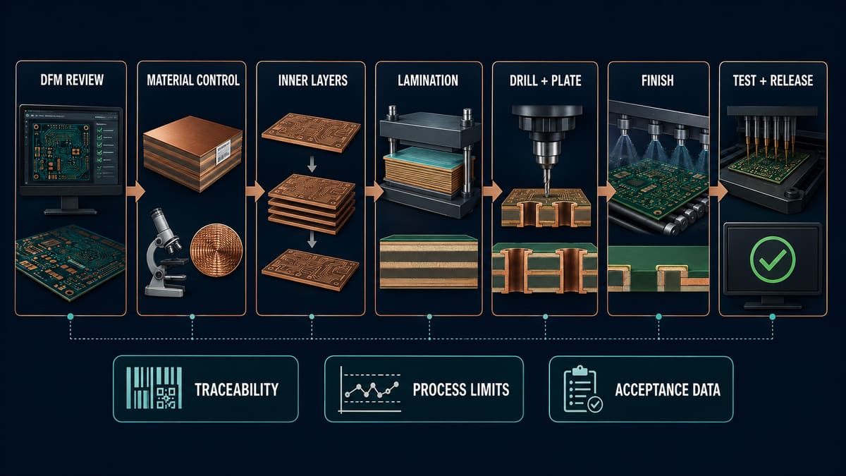
The continuous fabrication flow below applies to a typical multilayer industrial board. Exact sequencing changes with structure, finish and special features, but every stage needs a defined control, a defect response and evidence that supports release.
1. Engineering review and tooling. CAM engineering checks data completeness, annular features, clearances, rout geometry, layer registration allowances and panelization. This prevents ambiguous data from becoming repeated scrap. Buyers should receive a question list or approved engineering change record rather than silent edits.
2. Material preparation. The factory selects and conditions laminate, copper foil and prepreg against the approved build. Material identity and lot control matter because resin behavior and copper thickness affect lamination, drilling and long-term interconnection performance. Unapproved substitution can invalidate earlier qualification logic.
3. Inner-layer imaging, etching and AOI. The circuit image is transferred to copper, unwanted copper is etched, and inner layers are inspected before they disappear into the stack. Under-etching, over-etching, contamination or image shift can produce shorts, opens or reduced conductor geometry. AOI findings should drive rework or rejection before lamination.
4. Lay-up and lamination. Inner cores and prepreg are aligned and pressed under a controlled thermal and pressure cycle. Resin flow, cure and registration must be stable. Poor control can cause voids, thickness variation, layer shift or weak bonding that final electrical test may not reveal.
5. Drilling, desmear and hole preparation. Mechanical or laser drilling creates vias and component holes. Tool condition, entry/backup materials and drilling parameters influence hole position and wall quality. Desmear removes resin residue and prepares exposed copper for metallization; incomplete preparation can lead to weak or intermittent plated connections.
6. Electroless copper and electrolytic plating. Conductive copper is established through holes and then built to the required structure. Chemistry, current distribution and panel design affect deposit consistency. Thin, rough or voided plating raises interconnect risk, so relevant projects may require coupon measurement or microsection evidence.
7. Outer-layer imaging and etching. The factory defines final outer conductors while protecting plated features. Fine spaces and copper distribution affect etching uniformity. Inspection checks conductor integrity and registration before solder mask covers the surface.
8. Solder mask, legend and surface finish. Mask protects conductors and defines exposed pads. Registration, cure and cleanliness influence assembly and insulation. The selected surface finish must match storage, soldering, contact and environmental needs rather than being treated as a cosmetic choice.
9. Profiling and final mechanical work. Routing, V-scoring or other separation operations create the final outline. Dimensional checks should include critical connector edges, slots and mounting features. Burrs, excessive stress or wrong dimensions can prevent enclosure fit even when the circuit is electrically sound.
10. Inspection, electrical test and release. Visual and dimensional inspection, continuity/isolation testing and project-specific evidence complete bare-board release. The supplier should link results to the correct part number, revision and lot. A test pass proves only the conditions covered by that test plan.
How Should Materials Be Selected for Industrial PCBs?
Material selection begins with operating stress, assembly profile and qualification history, not with a generic “high-grade FR-4” label. Define thermal exposure, voltage, frequency, moisture, mechanical loading, flammability or regulatory needs, then confirm that the complete stackup uses an approved material family.
If the supplier proposes an alternative, ask what electrical, thermal, mechanical and process characteristics were compared and whether the change affects impedance, drilling, plating, soldering or qualification. A similar headline Tg alone does not prove equivalence.
Which Process Controls Protect Long-Term Reliability?
The strongest controls prevent drift before final inspection. Useful evidence may include incoming material identification, controlled work instructions, calibrated measurements, chemistry monitoring, registration checks, AOI results, plating verification, dimensional reports, electrical-test records and nonconformance disposition. The exact package depends on risk.
Traceability must connect those records to the shipped lot. A certificate without a lot, revision or measured characteristic is weak evidence. Buyers should agree which records are supplied automatically, retained by the factory or available on request.
What Manufacturing Failures Should Engineers Watch For?
Failure analysis is most useful when each defect is linked to an upstream control and a buyer checkpoint.
| Failure signal | Possible process cause | Impact | Buyer checkpoint |
| Intermittent via | Smear, poor activation or plating discontinuity | Field opens after thermal stress | Hole preparation control and relevant microsection evidence |
| Layer misregistration | Material movement or imaging/lay-up error | Reduced annular margin or spacing | Registration inspection and coupon strategy |
| Delamination or blister | Moisture, contamination or cure problem | Assembly or service failure | Material handling and lamination records |
| Unexpected corrosion or leakage | Residue, poor rinse or incompatible surface protection | Insulation degradation | Cleanliness requirement and environmental validation |
| Mechanical fit failure | Profile, slot or thickness outside drawing | Assembly delay or connector stress | Critical-dimension report |
How Does PCB Design Affect Manufacturing Reliability?
Design determines how much process variation a board can tolerate. Marginal annular rings, abrupt copper imbalance, poorly defined high-current paths, tight edge clearances and ambiguous tolerances reduce the factory’s usable window. A design can pass a rules check yet remain fragile in production.
Review the layout against the actual stackup and supplier process before release. For industrial builds, also connect placement and enclosure constraints to vibration, thermal paths, connector load and coating keep-outs, even though those decisions extend beyond bare-board fabrication.
Which Tests Are Needed Before Industrial PCB Release?
Every bare-board lot normally needs an agreed continuity and isolation test, but electrical test cannot detect every material or structural weakness. Add inspection based on the failure mechanism you need to control.
- AOI finds image defects before buried layers are laminated.
- Dimensional inspection verifies outline, holes, slots and critical locations.
- Microsection analysis can examine plated-hole structure and layer registration when specified.
- Impedance coupons or measurements support controlled-impedance requirements.
- Cleanliness or environmental testing applies when contamination or service exposure is a defined risk.
- Assembly-level ICT or functional testing belongs to the PCBA test plan, not the bare-board electrical test.
Environmental validation should reproduce the application risk rather than add tests by habit. This PCB environmental testing overview can help frame the discussion, but the project specification must define the actual method and acceptance boundary.
How Should Prototypes Transfer to Volume Production?
A working prototype is evidence about the design, not automatic proof that the volume process is controlled. Before scale-up, freeze the data revision, approved stackup and materials, critical process notes, acceptance plan, test coverage, panelization, serialization or traceability needs and change-approval route.
Compare the prototype and production routes. A change in factory, material, panel, tooling or test method may require review or requalification. The buyer should define which changes need written approval before implementation.
What Evidence Should a Supplier Provide?
Ask for evidence that matches the project’s risk rather than a generic factory presentation. The useful question is “What record proves this requirement for my lot?”
- Approved stackup and material declaration tied to revision.
- Recorded disposition of CAM/DFM questions and deviations.
- Lot-level electrical-test status and applicable inspection reports.
- Critical dimension, impedance, coupon or microsection data when specified.
- Nonconformance and corrective-action process.
- Written control for material, process and production-site changes.
How Long Does Industrial PCB Manufacturing Take?
Lead time depends on layer count, material availability, drilling/plating complexity, finish, inspection evidence, quantity and engineering-response time. Prototype, small-batch and volume schedules should not be quoted from a generic table when the build includes special material, coupons, controlled impedance or qualification activity.
Ask the supplier to separate engineering review, material procurement, fabrication, special testing and shipping. A complete, contradiction-free release package often removes more schedule risk than demanding an aggressive production promise.
How Do You Choose an Industrial PCB Manufacturer?
Choose a manufacturer by process fit, engineering communication and evidence discipline. Confirm that the factory can review your stackup, explain exceptions, control the required materials and features, perform the agreed inspections, retain traceability and manage changes. Certifications can support a quality system, but they do not replace project-specific capability and records.
What Should Be Included in the RFQ and Release Checklist?
Use the same controlled package for every supplier so quotations are comparable.
- Step 1: Send Gerber, drill and netlist data with one revision identifier.
- Step 2: Add the stackup, fabrication drawing, material, copper and finish requirements.
- Step 3: State quantity, panel/delivery form and prototype-to-volume plan.
- Step 4: Define critical dimensions, impedance and acceptance evidence.
- Step 5: Describe operating stresses that affect material or qualification choices.
- Step 6: Require written approval for substitutions, deviations and material/process changes.
- Step 7: Compare quotations by scope, exclusions and evidence—not unit price alone.
Frequently Asked Questions
Is an industrial PCB a specific IPC class?
No. “Industrial” describes an application context, while an acceptance class or standard must be specified separately. Select requirements from the product risk and contract documents instead of assuming the word industrial creates a universal inspection level.
Does electrical test prove an industrial PCB is reliable?
Electrical test checks continuity and isolation under defined conditions. It does not by itself prove laminate identity, plating robustness, cleanliness, dimensional fit or resistance to thermal cycling. Combine it with risk-based process and inspection evidence.
What files are needed for an industrial PCB quote?
Provide Gerber data, NC drill files, stackup, fabrication drawing, quantity and delivery form. Add material, copper, finish, impedance, critical dimensions, special inspection and traceability requirements so suppliers price the same scope.
Can a supplier substitute an equivalent laminate?
Only under the agreed change-control rule. Compare the characteristics that affect your electrical, thermal, mechanical and manufacturing requirements, then document approval before production. A matching headline Tg is not enough evidence.
When is a microsection useful?
A microsection can support evaluation of plated-hole structure, copper distribution and registration when those characteristics matter to the build. Define sampling, location and acceptance requirements in advance rather than requesting an undefined “microsection report.”
What causes industrial PCB lead-time changes?
Common drivers include special material procurement, complex drilling/plating, engineering questions, controlled impedance, coupons, added inspection and quantity. Ask for a schedule broken into review, material, fabrication, testing and logistics.
Should prototype and volume boards use the same process?
They should use a controlled, understood baseline when the prototype is intended to qualify volume production. If factory, material, panelization, tooling or testing changes, review whether new validation is needed before approving volume release.
How should buyers compare industrial PCB suppliers?
Compare process compatibility, engineering response, material/change control, inspection scope, traceability and nonconformance handling. Send an identical RFQ package and ask each supplier to identify assumptions and exclusions in writing.
Request an Engineering Review
For an industrial PCB review, send PCBtry your Gerber files, drill files, stackup, fabrication drawing, quantity, application conditions and required acceptance evidence through the contact page. The review can identify data conflicts, manufacturing limits and test-scope gaps before they become production changes.



0 Comments