




What Is the Rigid-Flex PCB Manufacturing Process?
The rigid-flex PCB manufacturing process combines flexible polyimide circuits and rigid multilayer sections into one permanently laminated board. It is used when an electronic assembly needs fixed component areas plus an integrated circuit that folds or moves through a confined space. Unlike a rigid PCB connected by a separate cable, the plated interconnections, flexible conductors and rigid sections are fabricated as one structure, so material movement, bend geometry and the rigid-to-flex transition must be controlled together.
PCBTRY supports rigid-flex projects with stack-up review, DFM feedback, bare-board fabrication and assembly coordination. For an engineering assessment, send Gerber or ODB++ data, NC drill files, the proposed stack-up, bend drawing, finished thickness, surface finish, quantity and acceptance requirements through our contact page. The useful question is not only whether a supplier offers rigid-flex boards, but whether its qualified process matches your materials, via structure and bend conditions.
How Does the Rigid-Flex PCB Manufacturing Process Work?
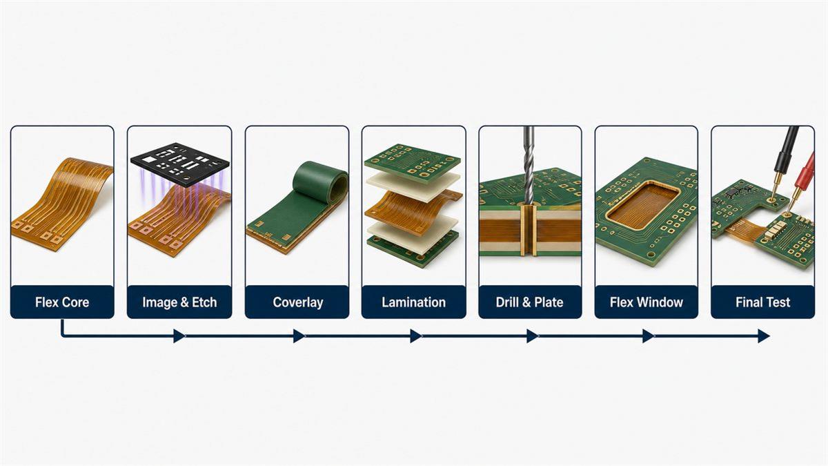
Rigid-flex fabrication builds and protects the flexible circuit first, integrates it with the rigid sections, completes common drilling and plating, then opens the flex windows without damaging the circuit below. The exact sequence changes with layer count, via structure, adhesiveless or adhesive-based materials, stiffeners and whether the flex area bends once or cycles repeatedly.
1. Engineering review and DFM release. CAM engineers compare the fabrication data, drill files, stack-up and mechanical drawing. They identify rigid, transition and active-bend zones; check coverlay openings, stiffeners, copper-to-edge spacing, tooling and controlled-impedance structures; and confirm which features must survive repeated bending. If the bend drawing and copper data disagree, manufacturing cannot safely infer the intended geometry. Review how to prepare Gerber files for PCB manufacturing before release.
2. Flexible core imaging and etching. Copper on the polyimide core is cleaned, imaged, developed and etched to form the flexible conductors. Thin material can stretch, shrink or move during handling, so artwork compensation, panel support and registration targets matter. Over-etching can reduce conductor width; rough handling can introduce creases that later concentrate strain.
3. Coverlay, access openings and stiffener preparation. Patterned polyimide coverlay protects the flex conductors while leaving pads and contacts exposed. Openings must align without reducing pad access or exposing unintended copper. Stiffeners and local support features are prepared for connector, component or contact regions, but their edges must not terminate where repeated bending will concentrate stress.
4. Rigid inner layers and subassembly preparation. Rigid cores are imaged, etched and inspected before integration. The factory also prepares no-flow or controlled-flow bonding materials and routed clearance areas that will later become flex windows. Inner-layer AOI is valuable here because an open or short becomes inaccessible after final lamination.
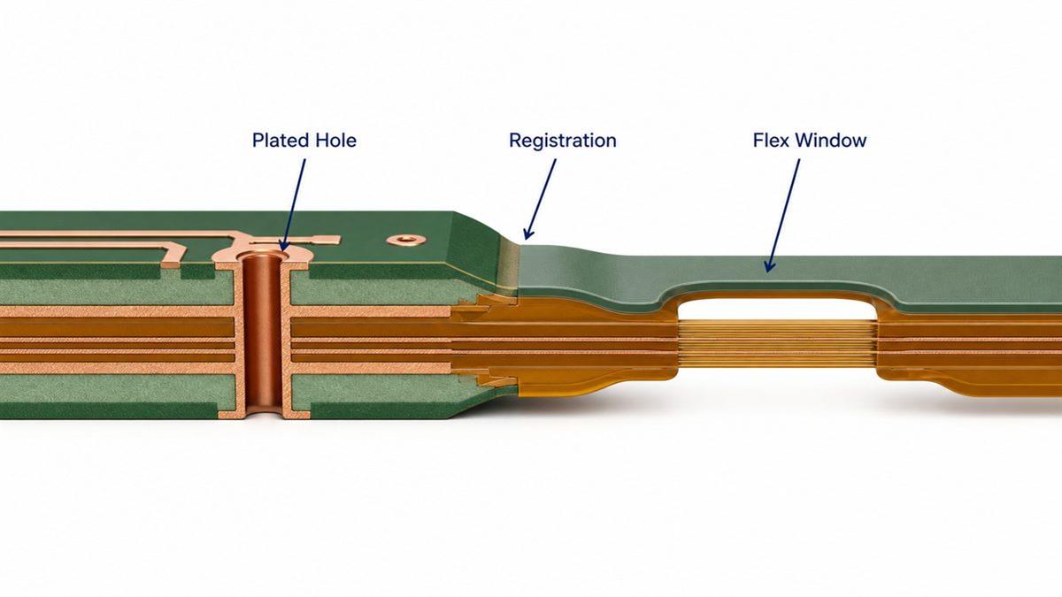
5. Registration and rigid-flex lamination. Flexible layers, rigid cores, bonding films and copper foils are aligned and pressed under a qualified temperature, pressure and vacuum cycle. Resin must bond the rigid sections without flowing into active flex areas or creating unstable transition geometry. Layer shift can reduce annular features, move a drilled hole away from its target or misalign the future flex window.
6. Drilling, plasma preparation and copper plating. Mechanical or laser drilling creates the specified interconnections. Hole walls may expose glass-reinforced epoxy, adhesive and polyimide, which do not respond identically to ordinary rigid-board desmear. Plasma or another qualified preparation method removes residue and conditions the mixed-material wall before electroless copper and electroplating. Inadequate preparation can create weak interfaces or intermittent barrels that pass a basic continuity check but fail after thermal or mechanical stress.
7. Outer-layer completion and flex-window opening. The outer circuitry is imaged and etched, followed by solder mask on rigid zones, surface finish, legend and final profiling. Controlled-depth routing, laser processing or approved tooling removes rigid material above the flex region. Cutting too deep can score the polyimide or copper; leaving residue can restrict movement and damage the transition during forming.
8. Inspection, electrical test and final handling. The finished board is checked against the released drawing and net data. Dimensional inspection, electrical continuity/isolation, microsections, impedance coupons and specified bend or thermal tests provide different evidence. Packaging must support the rigid sections and avoid uncontrolled folds, scratches and moisture exposure.
What Materials Are Used in Rigid-Flex PCB Manufacturing?
A rigid-flex material system must provide electrical insulation, adhesion, dimensional stability and the required bending behavior through repeated fabrication heat cycles. Material names alone are not enough; thickness, copper type, adhesive construction and bonding flow must be released as one stack-up.
| Material | Manufacturing role | Engineering check | Risk if mismatched |
|---|---|---|---|
| Polyimide flex dielectric | Supports conductors through bend areas | Thickness, adhesive construction, thermal and flex requirement | Unexpected stiffness, movement or delamination |
| Copper foil | Carries signals and power across rigid and flex zones | Weight, finished width and static/dynamic bend use | Cracking or excessive stiffness in the bend |
| Coverlay | Protects flexible copper and defines exposed pads | Opening registration, adhesive flow and bend coverage | Blocked pads, exposed copper or local stress |
| Rigid laminate | Supports components, holes and dense routing | Tg, CTE, thickness and electrical properties | Warp, registration shift or thermal mismatch |
| Bonding film / no-flow prepreg | Joins rigid and flex subassemblies | Flow behavior, cured thickness and lamination cycle | Resin intrusion, voids or poor transition geometry |
| Stiffener material | Supports connectors, contacts or component regions | Material, thickness, adhesive and edge location | Peel stress or a stiffness step near the bend |
Do not specify the flex layer with a generic note such as “Kapton” and leave the rest to interpretation. The fabrication drawing should identify the construction or reference an approved manufacturer stack-up.
How Is a Rigid-Flex PCB Stack-Up Designed?
A reliable stack-up begins with the mechanical use of the flex section, then adds only the layers needed for routing, reference planes, impedance and component support. Start by classifying each bend as installation-only or dynamic. Mark the bend direction, angle, available radius and transition boundaries before locking the layer count.
The designer and fabricator should then agree on the rigid layer build, flexible copper layers, coverlay, bonding materials, finished thickness, copper balance, via structure and impedance references. A symmetric rigid construction may help control warpage, but the complete hybrid structure—not a rigid-board template—must be assessed. See how multilayer stack-up and lamination decisions interact.
- Define rigid, transition and active-bend zones in the mechanical drawing.
- Keep plated holes, component pads and abrupt copper changes out of active bends.
- Confirm which flex layers continue through each rigid section.
- State impedance targets and the layers that form each reference structure.
- Release material thicknesses and finished board thickness with realistic tolerances.
- Ask the fabricator to return an approved production stack-up before tooling.
What Are the Key Manufacturing Challenges?
The hardest rigid-flex controls occur where thin flexible materials must stay registered and undamaged while being processed with thicker rigid materials. These risks interact: a small lamination shift can reduce hole registration, and a poorly controlled window operation can turn an electrically good panel into a mechanically unreliable part.
| Challenge | What can fail | Process control | Evidence to request |
|---|---|---|---|
| Flex-layer movement | Pad, coverlay or hole misregistration | Panel support, targets and material-specific compensation | Registration records and dimensional results |
| Resin flow at transition | Stiffened bend, void or irregular edge | Qualified bonding material and lamination cycle | Transition inspection or approved section |
| Mixed-material hole wall | Residue, weak copper interface or barrel failure | Qualified plasma/desmear and plating process | Microsection and plating acceptance data |
| Flex-window removal | Scored polyimide, damaged copper or residual rigid material | Controlled-depth tooling and protected support | Window-edge inspection and first-article dimensions |
| Final handling | Creases, scratches or uncontrolled pre-forming | Defined fixtures, packing and bend protection | Packaging plan and outgoing inspection |
How Does Design Affect Rigid-Flex Reliability?
Manufacturing cannot remove a stress concentration that is built into the copper or mechanical geometry. The design should route conductors smoothly through active bends, avoid abrupt width changes, and keep vias, component pads, stiffener edges and rigid-window edges away from the moving region.
For dynamic bending, conductor orientation, copper construction, total flex thickness and layer count all affect fatigue behavior. For installation-only bends, the main risk may be damage during forming or assembly rather than lifetime cycling. Ask the supplier to validate the proposed stack-up and bend condition instead of applying one generic bend-radius ratio to every construction. If the project is still deciding between flex and rigid-flex, review what flexible PCBs are and where a separate rigid section may be simpler.
What Tests Verify Rigid-Flex PCB Quality?
No single test proves rigid-flex reliability. Electrical test verifies the netlist, while dimensional, cross-sectional and mechanical evidence checks the structures that create long-term risk.
| Inspection or test | What it verifies | What it does not prove alone |
|---|---|---|
| Inner-layer AOI | Opens, shorts and pattern defects before lamination | Final plated-hole or flex-window quality |
| Final electrical test | Continuity and isolation against net data | Fatigue life or a marginal plating interface |
| Dimensional inspection | Outline, holes, openings, stiffeners and critical positions | Internal adhesion or copper thickness |
| Microsection / coupon | Hole-wall preparation, plating, registration and interfaces | The condition of every feature unless sampling is defined |
| Impedance coupon test | Specified controlled-impedance structures | All signal-integrity behavior in the assembled product |
| Bend or thermal testing | Performance under a defined mechanical or thermal condition | Service life when the test profile does not match use |
The purchase drawing should define which evidence is required and how acceptance will be judged. A supplier capability sheet is not a substitute for lot-specific results. PCBTRY’s PCB testing guide explains how different tests answer different questions.
How Long Does Rigid-Flex PCB Manufacturing Take?
Rigid-flex boards generally need more engineering and process time than comparable rigid multilayer boards because the stack-up, bend zones, coverlay, bonding materials, lamination cycle, flex windows and test plan require additional review and tooling. A prototype with a mature, previously qualified construction will usually move faster than a new multilayer build with unusual materials or dynamic-bend qualification.
Lead time is affected by material availability, layer count, number of lamination cycles, via type, impedance requirements, stiffeners, surface finish, coupon testing, first-article approval and assembly scope. For a meaningful schedule, submit the complete release package and ask the supplier to separate engineering review, material procurement, fabrication, special testing and assembly time.
What Should Be Included in a Rigid-Flex PCB RFQ?
A complete RFQ lets the manufacturer price the real construction instead of adding assumptions that later become engineering changes.
- Gerber or ODB++ data plus NC drill and route files.
- Fabrication drawing with rigid/flex boundaries, stack-up, materials, copper, thickness, finish and tolerances.
- Bend drawing showing direction, angle, radius, installed shape and static or dynamic use.
- Impedance table and any required coupons.
- Stiffener, coverlay, shielding and exposed-contact requirements.
- IPC-356 or another approved netlist reference when available.
- Quantity, panel or delivery format and prototype/production forecast.
- Inspection reports, microsections, certificates or reliability tests required for acceptance.
- BOM, CPL/centroid, assembly drawing and test requirements when PCBA is included.
How Do You Choose a Rigid-Flex PCB Manufacturer?
Choose a supplier by matching its qualified construction, engineering support and test evidence to your design—not by comparing a maximum layer-count table alone. A useful review starts with the actual stack-up and bend drawing.
- Can the engineering team identify transition zones, active bends and coverlay/stiffener conflicts during DFM?
- Which material systems and bonding processes are qualified for this construction?
- How are thin flex layers supported and registered during imaging and lamination?
- How are mixed polyimide, adhesive and epoxy hole walls prepared before plating?
- How is the flex window opened, inspected and protected during handling?
- Which lot-specific electrical, dimensional, microsection, impedance or mechanical records are available?
- Can the supplier support prototype learning and preserve the approved stack-up for production?
Use the rigid-flex PCB manufacturing page to compare project requirements with PCBTRY’s service scope, then request written confirmation for every critical construction and acceptance item.
Frequently Asked Questions About Rigid-Flex PCB Manufacturing
What is the difference between a flex PCB and a rigid-flex PCB?
A flex PCB is built primarily from flexible materials. A rigid-flex PCB permanently integrates rigid multilayer sections and flexible interconnect sections, so components can be supported on rigid areas while the same circuit bends between them.
Is rigid-flex fabricated before components are assembled?
Yes. The integrated bare board is fabricated and electrically tested first. Component assembly, reflow, AOI, X-ray and functional testing are downstream processes that require additional fixtures and handling controls.
Why is plasma treatment used in rigid-flex fabrication?
Drilled holes may expose polyimide, adhesive and rigid laminate. A qualified plasma process can remove residue and condition these mixed surfaces before copper deposition, improving the chance of a sound plated interface.
Can rigid-flex boards support dynamic bending?
They can when the materials, copper, thickness, layer count, bend geometry and test plan are designed for repeated motion. A construction intended to fold once during installation should not automatically be treated as a dynamic-flex design.
What causes rigid-flex delamination?
Possible causes include contamination, moisture, incompatible materials, inadequate surface preparation, trapped voids or an incorrect lamination cycle. Failure analysis should identify the interface and process condition rather than treating every separation as the same defect.
How is a rigid-flex PCB electrically tested?
A flying-probe or fixture test can check continuity and isolation against the released net data. The correct method depends on quantity, density, access and acceptance requirements; electrical test does not replace cross-sectional or mechanical evidence.
What makes rigid-flex PCBs more expensive than rigid PCBs?
Specialized flex materials, coverlay and stiffeners, extra engineering, material handling, lamination, mixed-material hole preparation, controlled window opening, lower panel utilization and additional inspection can all affect cost.
What files are needed for a rigid-flex quotation?
Send fabrication and drill data, a stack-up/fabrication drawing, bend information, materials, finish, impedance, quantity and acceptance requirements. Add BOM, CPL, assembly drawings and test details when assembled boards are required.
Request a Rigid-Flex DFM Review
Before releasing a prototype or production order, send PCBTRY the fabrication data, drill files, stack-up, bend drawing, material and finish requirements, quantity and test plan through the contact page. Ask for written confirmation of the transition geometry, coverlay and stiffeners, hole preparation, flex-window method and required inspection evidence so the quotation reflects the board you actually intend to build.



0 Comments