




PCB testing is the process of checking a printed circuit board for electrical defects, manufacturing errors, assembly problems and reliability risks before it is used in a final product. A board can look clean from the outside and still have hidden issues such as open circuits, short circuits, poor solder joints, impedance deviation, weak vias or component placement errors.
For engineers and buyers, PCB testing is not just a final quality step. It helps reduce field failures, protect product schedules, improve manufacturing yield and confirm that a design can move safely from prototype to mass production.
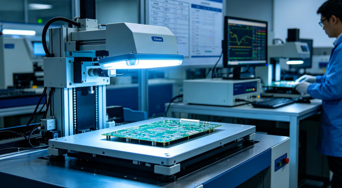
What Is PCB Testing?
PCB testing verifies whether a bare PCB or assembled PCBA meets its electrical, mechanical, visual and reliability requirements.
In bare board production, testing usually focuses on continuity, isolation, dimensions, copper quality, hole quality, solder mask alignment, surface finish and impedance control. In PCBA production, testing becomes broader because the board already contains components, solder joints, connectors and functional circuits.
A complete testing plan may include visual inspection, automated optical inspection, X-ray inspection, electrical test, impedance testing, in-circuit testing, flying probe testing, functional testing, burn-in testing and reliability checks. The right combination depends on board complexity, application risk, production volume and customer requirements.
Why PCB Testing Matters
PCB testing matters because many board failures are cheaper to catch during manufacturing than after shipment, assembly or field use.
A small defect can become a serious product issue. A cracked via may pass a simple power-on check but fail after thermal cycling. A solder bridge may damage an IC. A wrong component value may cause unstable performance. Poor impedance control can create signal integrity problems in high-speed communication products.
For consumer electronics, testing helps control cost and delivery consistency. For automotive, medical, industrial, communication and power electronics, it also supports long-term reliability and compliance expectations. In these industries, a board is rarely judged only by whether it works once. It must keep working under heat, vibration, humidity, current load and repeated operation.
How PCB Testing Works in Manufacturing
PCB testing works by checking the board at several points instead of waiting until the end of production.
A typical process starts with incoming material control, then moves through inner layer inspection, lamination checks, drilling inspection, plating checks, solder mask inspection, surface finish inspection and final electrical test. For assembled PCBAs, additional steps include solder paste inspection, component verification, AOI, X-ray inspection, ICT, flying probe testing and functional testing.
This staged approach is important because different defects appear at different production stages. Inner-layer shorts must be found before lamination. Plating voids must be controlled before final finishing. Soldering defects must be caught after assembly. Functional issues must be confirmed after the board is powered and operated under defined conditions.
| Production Stage | Main Testing Focus | Common Defects Found | Why It Matters |
|---|---|---|---|
| Incoming material inspection | Laminate, copper foil, solder mask and surface finish material checks | Wrong material, damaged laminate, poor storage condition | Prevents unstable quality before fabrication begins |
| Inner layer inspection | Trace width, spacing, shorts, opens and registration | Etching errors, inner-layer shorts, misalignment | Defects become difficult or impossible to repair after lamination |
| Drilling and plating inspection | Hole size, wall quality, copper thickness and via reliability | Hole breakout, plating voids, thin copper, rough hole walls | Via failure is one of the most serious reliability risks |
| Final bare board test | Continuity, isolation, impedance and final appearance | Open circuits, short circuits, impedance deviation, solder mask defects | Confirms the PCB is ready for assembly |
| PCBA inspection | Solder joints, polarity, component placement and hidden joints | Tombstoning, bridges, voids, missing parts, reversed components | Reduces assembly-related failures before functional testing |
| Functional testing | Real circuit operation under defined conditions | Firmware issues, unstable output, power faults, communication failure | Confirms whether the assembled board performs as intended |
Common PCB Testing Methods
Common PCB testing methods include visual inspection, AOI, X-ray inspection, electrical testing, ICT, flying probe testing and functional testing.
No single test method can catch every problem. A simple two-layer bare board may only need visual inspection and electrical test. A dense BGA assembly may require AOI, X-ray and functional testing. A high-speed board may need impedance testing and careful stack-up verification. A power board may require current, insulation and thermal checks.
| Testing Method | What It Checks | Best Use Case | Limitation |
|---|---|---|---|
| Visual inspection | Surface defects, scratches, solder mask issues, obvious assembly errors | All PCB and PCBA production stages | Depends on inspector experience and cannot detect hidden defects |
| AOI | Trace defects, solder joint shape, missing parts, wrong placement, polarity issues | SMT assembly and high-volume PCBA production | May miss hidden joints under BGA or bottom-terminated components |
| X-ray inspection | Hidden solder joints, BGA voids, internal bridges and solder coverage | BGA, QFN, dense assemblies and high-reliability PCBAs | Higher cost and usually requires trained interpretation |
| Electrical test | Open circuits, short circuits, continuity and isolation | Bare PCB testing before shipment or assembly | Does not verify circuit function after components are installed |
| Flying probe test | Net connectivity, component values and basic electrical behavior | Prototypes, small batches and boards without test fixtures | Slower than fixture-based ICT for large production runs |
| ICT | Component values, solder quality, shorts, opens and node-level electrical checks | Medium- to high-volume PCBA production | Requires test fixture design and enough test access points |
| Functional test | Real operating performance of the assembled board | Power supplies, control boards, communication modules and finished PCBAs | Test coverage depends on fixture quality and test procedure design |
Bare PCB Testing vs PCBA Testing
Bare PCB testing checks the fabricated board before components are assembled, while PCBA testing checks the assembled circuit after soldering and component placement.
Bare board testing is mainly about whether the copper network is correct and manufacturable. It checks opens, shorts, hole quality, surface condition, solder mask, dimensions and sometimes controlled impedance. PCBA testing adds another layer of risk because components, solder joints, polarity, firmware and real circuit behavior all become part of the quality result.
| Item | Bare PCB Testing | PCBA Testing |
|---|---|---|
| Main purpose | Verify board fabrication quality | Verify assembly quality and circuit function |
| Typical tests | Electrical test, visual inspection, impedance test, dimensional inspection | AOI, X-ray, ICT, flying probe, functional test, burn-in test |
| Common defects | Opens, shorts, plating defects, solder mask shift, impedance deviation | Solder bridges, missing parts, wrong polarity, BGA voids, functional failure |
| Best timing | Before assembly | After SMT, THT or mixed assembly |
| Procurement value | Prevents bad boards from entering assembly | Prevents defective assemblies from reaching final products |
Key PCB Inspection Methods and What They Reveal
PCB inspection methods reveal different types of defects, so reliable quality control usually combines optical, electrical and process-based checks.
Visual inspection is still useful because trained operators can identify contamination, scratches, solder mask defects, poor silkscreen, exposed copper and handling damage. AOI improves consistency by comparing board images against programmed references. X-ray inspection is valuable when solder joints are hidden under components.
For high-density, high-speed or high-reliability boards, inspection should not stop at appearance. The manufacturer may also check microsection samples, copper plating quality, hole wall integrity, solderability, ionic cleanliness, impedance coupons and dimensional stability. These tests help catch problems that may not be visible on the finished surface.
Electrical Testing for Bare PCBs
Electrical testing for bare PCBs confirms that every required net is connected and separated from other nets as designed.
The two basic checks are continuity and isolation. Continuity testing verifies that connected points are electrically linked. Isolation testing checks that separate nets do not accidentally short together. For many bare boards, this is the final gate before shipment or assembly.
Electrical test is especially important for multilayer boards, HDI boards, fine-pitch layouts, dense vias and boards with narrow spacing. As routing density increases, small etching or plating defects become harder to detect visually. Electrical testing helps catch those issues before they become expensive assembly failures.
| Parameter | What It Means | Suitable Scenario | Relative Cost | Limitation |
|---|---|---|---|---|
| Continuity test | Confirms required copper paths are connected | All bare PCBs | Low to medium | Does not prove final circuit function |
| Isolation test | Confirms separate nets are not shorted | Fine-pitch, multilayer and high-density boards | Low to medium | Cannot identify all material reliability risks |
| Controlled impedance test | Checks impedance against design requirements | High-speed, RF, communication and server boards | Medium | Requires correct stack-up, trace geometry and test coupons |
| Hi-pot test | Checks insulation strength under higher voltage | Power electronics, chargers, industrial equipment | Medium | Test conditions must match product safety requirements |
PCBA Testing After Assembly
PCBA testing verifies that components are correctly assembled and that the board performs its intended electrical function.
Assembly introduces many new risks. Components may be missing, shifted, reversed or incorrectly substituted. Solder joints may bridge, crack, void or remain insufficiently wetted. Connectors may be misaligned. Firmware may not load correctly. A board may pass visual inspection but still fail under real operation.
A practical PCBA testing plan often includes solder paste inspection before reflow, AOI after SMT, X-ray for hidden solder joints, ICT or flying probe for electrical coverage, and functional testing for real operation. For high-reliability applications, burn-in or stress testing may also be used to screen early-life failures.
PCB Testing Standards and Quality References
PCB testing standards help manufacturers, engineers and buyers use the same quality language when judging board acceptability.
Common references include IPC-A-600 for printed board acceptability, IPC-6012 for rigid printed board qualification and performance, IPC-A-610 for electronic assembly acceptability, and J-STD-001 for soldered electrical and electronic assemblies. UL recognition and RoHS compliance may also be required depending on product category and market requirements.
Thindry manufactures PCBs and PCBAs under internationally recognized quality systems, including ISO 9001, ISO 13485, IATF 16949, UL certification and RoHS compliance. These certifications are especially important for customers working on medical electronics, automotive electronics, industrial systems and export-oriented products.
| Standard or Certification | Main Focus | Typical Relevance |
|---|---|---|
| IPC-A-600 | Acceptability of printed boards | Bare PCB visual and structural quality |
| IPC-6012 | Qualification and performance for rigid PCBs | Rigid PCB manufacturing requirements |
| IPC-A-610 | Acceptability of electronic assemblies | PCBA soldering and assembly quality |
| J-STD-001 | Soldered electrical and electronic assemblies | Assembly workmanship and soldering process control |
| ISO 9001 | Quality management system | General manufacturing quality control |
| ISO 13485 | Medical device quality management | Medical PCB and PCBA projects |
| IATF 16949 | Automotive quality management | Automotive-grade electronics manufacturing |
| RoHS | Restriction of hazardous substances | Environmentally compliant electronics |
Common PCB Defects Found During Testing
Common PCB defects include open circuits, short circuits, plating voids, solder bridges, insufficient solder, wrong components, impedance deviation and hidden BGA defects.
Some defects are caused by fabrication. Others come from assembly, handling, design constraints or incomplete test planning. Understanding the source of each defect helps engineers fix the root cause instead of only sorting failed boards.
| Defect | Possible Cause | How Testing Finds It | Engineering Risk |
|---|---|---|---|
| Open circuit | Over-etching, broken trace, drilling damage, plating failure | Electrical test, flying probe, ICT | Signal or power path failure |
| Short circuit | Under-etching, copper residue, solder bridge, design spacing issue | Electrical test, AOI, ICT | Component damage, power failure or unstable operation |
| Plating void | Poor hole preparation, contamination, plating process issue | Microsection, electrical test, reliability testing | Intermittent via failure after thermal stress |
| Solder bridge | Stencil issue, excessive solder paste, fine-pitch assembly challenge | AOI, X-ray, ICT | Shorted IC pins or circuit failure |
| Insufficient solder | Poor paste deposit, pad design issue, reflow process problem | AOI, X-ray, functional test | Weak joint and early field failure |
| Wrong polarity | Incorrect placement, BOM error, unclear silkscreen | AOI, ICT, functional test | Board does not start or component is damaged |
| Impedance deviation | Stack-up mismatch, trace width variation, material variation | Impedance testing with coupons | Signal reflection, data errors and reduced high-speed performance |
PCB Failure Analysis and Engineering Lessons
PCB failure analysis looks beyond the failed board and asks why the defect happened, whether it can repeat and how the process should be corrected.
In real production, many failures are not caused by one obvious mistake. A via crack may involve material selection, copper plating thickness, thermal expansion and reflow profile. A BGA solder issue may involve pad design, paste volume, warpage and reflow temperature. A field failure in a power board may involve current load, thermal path, copper thickness and insulation distance.
A good engineering review usually checks the Gerber files, stack-up, material type, copper thickness, drill structure, solder mask clearance, stencil design, BOM, reflow profile and test coverage. This is why experienced PCB manufacturers often review manufacturability before production instead of only testing after production.
- Do not rely only on final functional testing for complex PCBAs.
- Use test points early in the layout when ICT or flying probe testing is required.
- Confirm impedance requirements before stack-up approval, not after fabrication.
- For BGA and QFN packages, plan X-ray inspection when solder joints are hidden.
- For power boards, check creepage, clearance, copper thickness and heat rise.
- For automotive and industrial boards, consider thermal cycling and vibration risk.
How to Choose the Right PCB Testing Method
The right PCB testing method depends on board complexity, production volume, application risk, component package type and the cost of failure.
For a simple prototype, flying probe testing may be more practical than building a dedicated ICT fixture. For high-volume production, ICT can improve speed and consistency. For boards with BGA components, X-ray inspection becomes important. For finished control boards, functional testing is often the most meaningful final check.
| Project Type | Recommended Testing Approach | Reason | Key Risk to Check |
|---|---|---|---|
| Prototype PCB | Visual inspection, electrical test, flying probe | Flexible and does not require expensive fixtures | Design errors and first-build assembly issues |
| High-volume PCBA | AOI, ICT, functional test, process monitoring | Improves repeatability and production efficiency | Fixture coverage and false pass risk |
| BGA or QFN assembly | AOI, X-ray, functional test | Hidden solder joints cannot be fully checked visually | Voids, bridges and insufficient solder |
| High-speed PCB | Impedance testing, stack-up verification, electrical test | Signal quality depends on controlled geometry and material | Insertion loss, reflection and impedance deviation |
| Power electronics | Electrical test, Hi-pot test, functional load test, thermal review | High current and voltage create safety and heat risks | Insulation breakdown, overheating and copper capacity |
| Automotive electronics | AOI, X-ray if needed, ICT, functional test, reliability checks | Long life and harsh environments require stronger control | Thermal cycling, vibration and intermittent failure |
Design-for-Test Tips Before PCB Manufacturing
Design-for-test means planning test access, measurement points and inspection visibility before the PCB layout is locked.
Many testing problems are actually design problems. If there are no accessible test points, ICT coverage becomes limited. If components are placed too close together, AOI may struggle. If BGA escape routing is too dense, X-ray interpretation and rework become harder. If impedance rules are unclear, the manufacturer may not know which traces require controlled testing.
- Add clear test points for key power rails, ground, communication lines and programming interfaces.
- Keep enough spacing around critical components for inspection and rework access.
- Mark polarity clearly for diodes, electrolytic capacitors, connectors and ICs.
- Provide impedance requirements together with stack-up expectations.
- Separate high-current, high-voltage and sensitive signal areas properly.
- Use consistent BOM references and avoid unclear component substitutions.
- Discuss ICT, flying probe or functional test needs before mass production.
PCB Testing for Different Industries
PCB testing requirements change by industry because each application has different reliability, safety, thermal and performance expectations.
A wearable device may prioritize compact structure and FPC reliability. An automotive controller may require wide-temperature performance and vibration resistance. A communication board may need impedance and signal integrity control. A power inverter may need high-current, high-voltage and thermal testing.
| Industry | Typical Products | Common PCB Types | Testing Priorities |
|---|---|---|---|
| Consumer electronics | Smart TVs, wearables, cameras, smart home devices, game consoles | HDI PCB, FPC, rigid-flex PCB, single-sided and double-sided PCB | AOI, electrical test, functional test, cost-effective yield control |
| Automotive electronics | BMS, VCU, MCU, OBC, ADAS, radar, camera modules, lighting control | Thick copper PCB, high-frequency PCB, metal core PCB, HDI, FPC | IATF-related quality control, thermal reliability, vibration risk, functional stability |
| Communication equipment | 5G modules, optical modules, routers, switches, server backplanes, RF front ends | High-frequency PCB, high-speed PCB, multilayer PCB, HDI | Impedance control, signal integrity, low-loss material verification, X-ray if needed |
| Servers and AI hardware | AI servers, GPU boards, FPGA accelerator cards, data center switches | High-layer-count PCB, high-speed backplane, low-loss material PCB | Impedance, flatness, registration, insertion-loss-related process control |
| Industrial control | PLC, servo drives, inverters, robotics, sensors, CNC systems, industrial gateways | Thick copper PCB, multilayer PCB, metal core PCB, double-sided PCB | Functional testing, EMC-related layout review, thermal control, long-life reliability |
| Medical electronics | Monitors, ultrasound systems, endoscopy, IVD devices, portable medical equipment | HDI, rigid-flex PCB, high-frequency PCB, metal core PCB | ISO 13485 quality control, low-noise operation, reliability and traceability |
| New energy and power electronics | PV inverters, energy storage converters, EV chargers, UPS power systems | Thick copper PCB, aluminum PCB, copper base PCB, multilayer PCB | Hi-pot test, current capacity, thermal rise, insulation distance and load testing |
| LED and lighting | Outdoor lighting, automotive lighting, plant lighting | Aluminum PCB, copper base PCB, FPC, single-sided and double-sided PCB | Thermal transfer, solder joint quality, surface finish and functional lighting test |
PCB Testing Cost Factors
PCB testing cost depends on test method, board complexity, volume, fixture requirements, component type and reliability expectations.
A bare board electrical test is usually much simpler than a full PCBA functional test. Flying probe testing is flexible for prototypes but slower for large batches. ICT is efficient for volume production but requires fixture investment. X-ray inspection adds cost but may be necessary for hidden solder joints. Burn-in and environmental testing require more time and equipment.
| Cost Factor | Why It Affects Price | How to Control It |
|---|---|---|
| Board complexity | Fine pitch, HDI, BGA and high-layer boards need more inspection effort | Review manufacturability before layout release |
| Test coverage | Higher coverage requires more equipment time and engineering setup | Define critical nets and real risk areas early |
| Fixture requirement | ICT and functional testing may need custom fixtures | Use fixtures for repeat production, not every early prototype |
| Production volume | Setup cost is easier to absorb in larger batches | Choose flying probe for small runs and fixture testing for stable volume |
| Reliability requirement | Automotive, medical and power boards often require stricter controls | Match tests to application risk instead of using a generic plan |
How to Choose a PCB Testing and Manufacturing Supplier
A reliable PCB testing supplier should understand fabrication, assembly, inspection, failure analysis and production scaling.
Buyers sometimes compare suppliers only by unit price, but testing capability can decide whether a project moves smoothly into production. A supplier with weak test planning may ship boards that pass basic checks but fail later during assembly, system integration or field operation.
Thindry was founded in 2005 and provides PCB fabrication, PCB prototype, PCB assembly, component sourcing and engineering support through a digitalized one-stop electronics platform. As a China-based source factory serving global customers, Thindry supports projects from early samples to mass production without claiming overseas factories, warehouses or local branches.
- Check whether the supplier supports both bare PCB testing and PCBA testing.
- Ask which inspection methods are available for your board type.
- Confirm relevant certifications such as ISO 9001, ISO 13485, IATF 16949, UL and RoHS when required.
- Review whether the supplier can support prototypes, engineering changes and volume production.
- Ask for manufacturability feedback before production starts.
- Make sure test reports, traceability and quality records can be provided when needed.
PCB Testing Checklist Before Placing an Order
A clear PCB testing checklist helps avoid misunderstandings between engineers, buyers and manufacturers before production begins.
| Checklist Item | What to Confirm | Why It Matters |
|---|---|---|
| Gerber and drill files | Latest revision, complete layers and correct drill data | Prevents production based on outdated or incomplete files |
| BOM and placement file | Correct part numbers, polarity and placement coordinates | Reduces assembly mistakes and wrong component use |
| Stack-up and impedance | Controlled impedance traces, material and layer structure | Protects signal performance in high-speed designs |
| Test method | Electrical test, AOI, X-ray, ICT, flying probe or functional test | Ensures the quality plan matches the application risk |
| Acceptance standard | IPC class, customer specification or special inspection criteria | Avoids disputes after production |
| Functional test procedure | Power input, test firmware, load condition and pass/fail criteria | Creates a repeatable PCBA testing process |
| Reporting requirement | Test report, inspection images, traceability or certificate documents | Supports internal quality review and customer audits |
FAQ About PCB Testing
What is the difference between PCB testing and PCB inspection?
PCB inspection usually refers to visual, optical, X-ray or dimensional checks, while PCB testing often includes electrical and functional verification. In practice, both are part of quality control. Inspection finds visible or structural defects, and testing confirms whether the board is electrically correct and able to perform as required.
Is electrical testing required for every PCB?
Electrical testing is strongly recommended for most bare PCBs, especially multilayer, HDI, fine-pitch and production boards. It checks continuity and isolation, helping catch opens and shorts before assembly. For very simple boards, some buyers may choose limited testing, but that increases assembly and field risk.
What is flying probe testing used for?
Flying probe testing is often used for prototypes, engineering samples and small batches because it does not require a dedicated test fixture. Moving probes contact test points or pads to check connectivity and some component values. It is flexible, but usually slower than ICT for high-volume production.
When should I choose ICT instead of flying probe testing?
ICT is a better choice when the PCBA design is stable and production volume is high enough to justify fixture cost. It is faster and more repeatable for volume testing. Flying probe is usually better for prototypes, design changes and smaller batches where fixture investment is not practical.
Why is X-ray inspection important for BGA components?
BGA solder joints are hidden under the component body, so they cannot be fully inspected by normal visual inspection or AOI. X-ray inspection helps identify solder bridges, voids, insufficient solder and alignment problems under BGA, QFN and other bottom-terminated packages.
Can a PCB pass electrical testing and still fail later?
Yes. Electrical testing can confirm opens and shorts at the time of test, but it may not reveal all long-term reliability risks. Problems such as weak vias, marginal solder joints, thermal stress, contamination or design-related heat issues may appear later during operation or environmental stress.
What is functional testing in PCBA manufacturing?
Functional testing powers the assembled board and checks whether it performs its intended operation. It may verify voltage outputs, current consumption, communication interfaces, sensors, relays, LEDs, firmware response or load behavior. A good functional test should have clear pass and fail criteria.
How much test coverage does a PCBA need?
Test coverage depends on product risk, volume, board complexity and failure cost. A simple consumer board may need AOI and functional testing, while automotive, medical, industrial or power electronics may need stronger coverage such as ICT, X-ray, burn-in or reliability checks.
What files are needed for PCBA testing?
The manufacturer typically needs Gerber files, drill files, BOM, pick-and-place files, schematic or netlist when applicable, test procedure, firmware, test limits and fixture requirements. For functional testing, the customer should also provide power conditions, expected outputs and any special operating steps.
Does PCB testing increase production cost?
PCB testing adds some cost, but it often reduces the total cost of failure. Finding a defect before shipment is much cheaper than repairing assembled boards, delaying production or handling field returns. The key is to choose testing methods that match the real product risk.
What standards are commonly used for PCB quality?
Common references include IPC-A-600 for bare PCB acceptability, IPC-6012 for rigid PCB performance, IPC-A-610 for electronic assemblies and J-STD-001 for soldered assemblies. Depending on industry needs, ISO 9001, ISO 13485, IATF 16949, UL and RoHS may also be important.
How can buyers avoid PCB testing disputes?
Buyers should confirm acceptance standards, test methods, reporting requirements and functional test criteria before placing an order. Ambiguous requirements often lead to disagreement later. Clear documentation, approved samples and revision control make testing results easier to judge and repeat.
What is the best PCB testing method?
There is no single best method for every project. Bare PCBs need electrical testing and inspection. Complex PCBAs may need AOI, X-ray, ICT, flying probe and functional testing. The best plan is the one that catches the most relevant risks without adding unnecessary cost or delay.
Final Thoughts on PCB Testing
Good PCB testing begins before production, not after problems appear. Engineers should design for test access, confirm stack-up and impedance needs, define functional test criteria and review manufacturing risks early. Buyers should choose a supplier that can support inspection, electrical testing, assembly testing, quality documentation and stable delivery from prototype to mass production.
Thindry supports PCB prototype, PCB fabrication, component sourcing and PCBA assembly for global customers across consumer electronics, automotive electronics, communication equipment, industrial control, medical electronics, new energy, LED lighting and other engineering applications.
If you’re sourcing reliable PCB/PCBA manufacturing — OEM, ODM, prototyping, mass production, or custom engineering solutions — reach out to our engineering team for technical support and a quote at [email protected].



0 Comments