




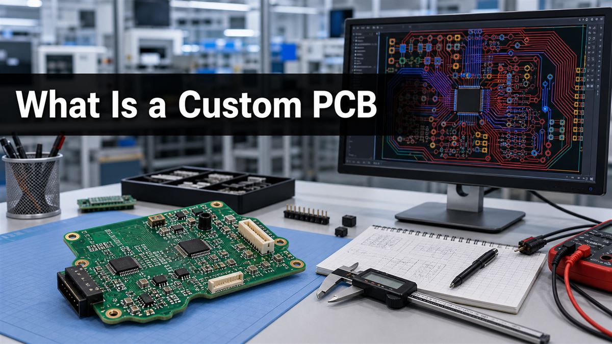
What Does Custom PCB Mean?
A custom PCB is a printed circuit board manufactured from project-specific design files rather than bought as a fixed, general-purpose board. The layout, dimensions, layer count, copper weight, material, solder mask, surface finish, hole structure, and test requirements are selected for one circuit and one use case.
In practical terms, a custom PCB turns an electronic design into a physical board that can hold components, route signals, distribute power, fit inside an enclosure, and survive the product’s operating conditions. It may be a simple 2-layer control board, a dense HDI board, a high-current power PCB, a rigid-flex board, or a small prototype used only for engineering validation.
The word “custom” does not automatically mean complex or expensive. It means the board is built to your data package. A simple custom PCB can be inexpensive if the design uses standard materials, common thickness, normal copper weight, and relaxed tolerances. Cost and lead time rise when the design needs special laminates, tight impedance, small vias, heavy copper, blind or buried vias, unusual thickness, or extra inspection.
How a Custom PCB Differs From a Standard PCB
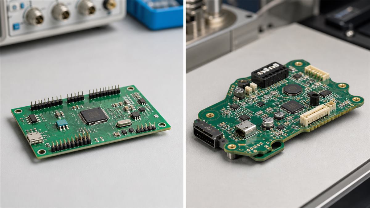
A standard PCB has a fixed format, while a custom PCB is shaped by the circuit, enclosure, electrical load, component package, and production requirement. Standard development boards are useful for learning, testing modules, or early proof-of-concept work, but they rarely match the final product’s size, connector position, thermal path, or compliance needs.
| Item | Standard PCB or Development Board | Custom PCB |
| Board outline | Fixed by the board supplier | Designed for the enclosure, connectors, mounting holes, and user interface |
| Circuit routing | Already defined | Designed for the actual schematic, component placement, and signal paths |
| Material and stackup | Usually fixed | Selected for mechanical, thermal, signal, cost, and production requirements |
| Production use | Best for evaluation and early testing | Best for prototypes, pilot runs, and finished products |
When Do You Need a Custom PCB?
You need a custom PCB when a ready-made board cannot meet the product’s electrical, mechanical, thermal, reliability, or production needs. This usually happens when the circuit must fit a defined space, connect to specific cables or sensors, carry higher current, handle controlled signals, or support automated assembly.
Typical cases include IoT devices, LED control boards, industrial controllers, power modules, medical electronics, automotive subassemblies, communication equipment, test fixtures, consumer devices, and embedded systems. A custom PCB is also useful when you want to reduce wiring, improve repeatability, simplify assembly, or move from a breadboard/prototype module to a manufacturable product.
One useful decision check is this: if the board shape, connector position, component placement, current path, signal quality, or production test method matters, the project has moved beyond a generic board.
What Information Defines a Custom PCB?
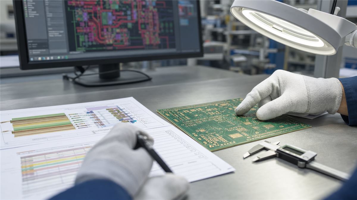
A custom PCB is defined by both design files and manufacturing notes. Gerber and drill files describe the physical copper, solder mask, silkscreen, board outline, and holes. The fabrication notes tell the manufacturer how the board should be built, inspected, and finished.
For a basic order, the manufacturer usually needs the Gerber files, NC drill file, board thickness, copper weight, surface finish, solder mask color, silkscreen color, quantity, and delivery requirement. For more demanding boards, you may also need a stackup drawing, impedance table, material requirement, via filling note, controlled depth drilling note, tolerance notes, and electrical test requirements.
| Information | Why It Matters | Common Risk If Missing |
| Gerber files | Define copper, solder mask, silkscreen, paste, and outline layers | Wrong layer interpretation or delayed engineering review |
| Drill file | Defines plated and non-plated holes | Wrong hole size, missing slots, or unclear plating requirement |
| Stackup | Defines layer order, dielectric structure, and thickness targets | Impedance, thickness, or lamination mismatch |
| Material requirement | Controls thermal, electrical, and mechanical behavior | Wrong laminate choice for heat, frequency, or reliability needs |
| Surface finish | Affects solderability, storage, flatness, and assembly fit | Poor match with fine-pitch, wire bonding, or shelf-life needs |
| Testing requirement | Defines electrical test, impedance test, or special inspection | Boards may pass basic checks but miss project-specific risks |
How Are Custom PCBs Manufactured?
Custom PCB manufacturing starts with engineering review, not with drilling or etching. The fabricator checks whether the files are complete, whether the layer count and stackup are clear, whether hole sizes match process capability, and whether any design details need confirmation before production.
After review, the usual fabrication flow includes material preparation, inner layer imaging and etching for multilayer boards, lamination, drilling, plating, outer layer imaging, copper pattern formation, solder mask, surface finish, legend printing, routing or V-cut, electrical test, final inspection, and packaging. The exact process changes with board type. HDI boards may need laser drilling and sequential lamination. Heavy copper boards need wider spacing and controlled plating. Rigid-flex boards need additional material and bend-area checks.
For this reason, two boards with the same outline size can have very different manufacturing difficulty. A 2-layer FR-4 prototype is usually straightforward. A small 8-layer board with impedance control, microvias, via-in-pad, and fine-pitch BGA escape routing needs tighter engineering review.
Which Design Choices Affect Cost and Lead Time?
Custom PCB cost and lead time are driven by process difficulty, not only by board area. Layer count, material type, copper weight, minimum line width and spacing, hole size, aspect ratio, surface finish, controlled impedance, via structures, tolerance requirements, and inspection level all affect the quote.
The most common cost drivers are extra layers, special laminate, heavy copper, small mechanical drills, laser vias, via filling, tight impedance tolerance, ENEPIG or hard gold finish, unusual board thickness, and tight routing tolerance. These choices may be necessary, but they should be tied to a real design requirement.
A practical way to control cost is to separate “must have” requirements from preferences. For example, if standard FR-4 meets the temperature and electrical need, do not specify a specialty laminate only because it sounds better. If ENIG is needed for fine-pitch assembly or shelf life, specify it. If HASL is enough for a simple through-hole board, it may be a better cost choice. Always verify material and process limits with the manufacturer before final production.
What Should Engineers Check Before Ordering?
Before ordering a custom PCB, engineers should check file completeness, design rule compliance, manufacturability, assembly fit, and test coverage. The goal is to catch preventable issues before the board enters fabrication.
- Confirm that Gerber, drill, outline, and stackup files match the same design revision.
- Check minimum trace width, spacing, hole size, annular ring, slot definition, and copper-to-edge clearance.
- Review connector locations, mounting holes, keep-out zones, board thickness, and enclosure fit.
- Verify high-current traces, thermal relief, copper balance, and heat-generating components.
- Confirm impedance requirements, differential pair routing, return paths, and reference planes where needed.
- Check whether the selected surface finish matches component pitch, storage, and assembly needs.
- Make sure special notes such as via filling, controlled depth routing, panelization, and electrical test are clear.
For assembled boards, also check the BOM, pick-and-place file, polarity marks, component lifecycle, package match, and test points. A board that is easy to fabricate can still be difficult to assemble if footprints, polarity, spacing, or component availability are not reviewed.
What Are Common Custom PCB Types?
Custom PCBs can be grouped by structure, material, performance requirement, or application. The right type depends on electrical load, density, bending requirement, operating temperature, signal frequency, and assembly method.
| Custom PCB Type | Typical Use | Engineering Note |
| Single-sided PCB | Simple controls, low-cost electronics, basic LED circuits | Limited routing space but easy to manufacture |
| Double-sided PCB | General electronics, power control, sensor boards | Good balance of routing flexibility and cost |
| Multilayer PCB | Dense circuits, signal integrity needs, compact products | Requires clear stackup and plane planning |
| HDI PCB | BGA routing, small devices, dense interconnects | May require laser vias and sequential lamination |
| Rigid-flex PCB | Folded products, moving assemblies, space-limited designs | Bend radius and flex material rules must be checked early |
| Metal core PCB | LED lighting and thermal management applications | Thermal path and dielectric selection affect performance |
How to Choose a Custom PCB Manufacturer
Choose a custom PCB manufacturer by matching your design difficulty with the factory’s verified process capability, engineering support, quality control, and communication speed. The lowest quote is not always the lowest total cost if unclear files, process mismatch, or weak inspection causes delays.
Ask whether the manufacturer can review DFM issues before production, confirm stackup and impedance requirements, support the required surface finish, provide electrical test, handle the target layer count and hole structure, and communicate engineering questions clearly. For production work, also ask about incoming material control, in-process inspection, final quality checks, traceability, packaging, and how nonconforming issues are handled.
If the project includes assembly, check whether the manufacturer can support PCB fabrication and PCBA together. This can reduce handoff errors between board fabrication, component sourcing, assembly, inspection, and functional testing.
FAQ About Custom PCBs
What does custom PCB mean?
A custom PCB is a printed circuit board made from project-specific design files. Its outline, layers, copper, material, finish, holes, and test requirements are selected for one circuit and application.
Is a custom PCB the same as a prototype PCB?
No. A prototype PCB is one stage of custom PCB production. A custom PCB can be a prototype, pilot run, or full production board.
What files are needed to order a custom PCB?
Most orders need Gerber files, drill files, board outline, board thickness, copper weight, surface finish, solder mask color, and quantity. Complex boards may also need stackup, impedance, material, and special process notes.
Can I order a custom PCB without a schematic?
A manufacturer can often fabricate from Gerber and drill files without the schematic, but the schematic helps with engineering review, assembly checks, and troubleshooting if something looks inconsistent.
How long does custom PCB manufacturing take?
Lead time depends on layer count, material, process difficulty, order quantity, testing, and engineering questions. Simple prototypes are faster than HDI, rigid-flex, heavy copper, or special-material boards.
What makes a custom PCB expensive?
Extra layers, special laminate, small holes, tight line spacing, heavy copper, controlled impedance, via filling, laser vias, unusual thickness, and special surface finishes can raise cost.
Which surface finish should I choose?
Choose the surface finish based on assembly method, component pitch, shelf life, flatness, and application needs. ENIG is common for fine-pitch assembly, while HASL may suit simpler boards. Verify the choice with the manufacturer.
Can a custom PCB be assembled with components?
Yes. Many custom PCBs can be ordered with assembly if you provide the BOM, pick-and-place file, assembly drawing, polarity notes, and test requirements.
What is DFM in custom PCB manufacturing?
DFM means design for manufacturability. It checks whether the PCB can be fabricated reliably with the selected process, material, hole sizes, spacing, copper, and tolerances.
Do custom PCBs need electrical testing?
Electrical testing is recommended for most custom PCBs because it checks opens and shorts before shipping. Some designs may also need impedance testing or additional inspection.
What is the difference between PCB fabrication and PCBA?
PCB fabrication makes the bare printed circuit board. PCBA adds components through SMT, through-hole assembly, soldering, inspection, and testing.
Can PCBTRY help review custom PCB files?
PCBTRY can review PCB manufacturing files and clarify fabrication or assembly requirements before production. For special materials, tight tolerances, impedance, or advanced structures, confirm capability before placing the order.
Final Takeaway
A custom PCB is the bridge between an electronic design and a manufacturable product. The best results come from clear files, realistic process choices, early DFM review, and a manufacturer that understands both fabrication and application requirements.
If you are preparing a custom PCB project, send your Gerber files, drill files, stackup notes, quantity, and special requirements to PCBTRY at [email protected]. The engineering team can help check manufacturability before production.



0 Comments