




High power components rarely fail because the schematic is wrong. More often, they fail because the heat has nowhere to go.
Power MOSFETs, LED drivers, DC-DC converters, motor driver ICs, GaN devices, voltage regulators, and high-current QFN packages can all generate concentrated heat in a very small area. If that heat remains trapped under the component, the result may be thermal shutdown, reduced efficiency, shortened lifetime, solder joint fatigue, or field failure.
Thermal vias are one of the most practical PCB-level tools for moving heat away from these components. A good thermal via design can lower the component temperature without dramatically increasing board size or adding expensive mechanical heat sinks. A poor design, however, can cause solder wicking, voiding, assembly defects, or provide much less cooling than expected.
This guide explains how to design thermal vias for high power components from a practical PCB manufacturing and layout perspective.
What Are Thermal Vias?
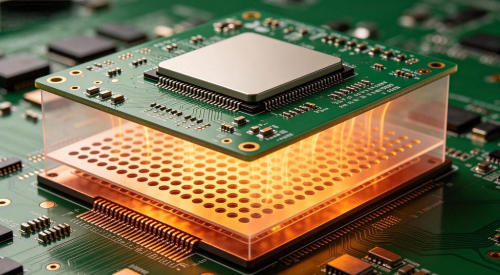
Thermal vias are plated holes used to conduct heat from one PCB layer to another. They are usually placed under or near a heat-generating component, connecting the top copper pad to internal copper planes, bottom-side copper areas, or external heat-spreading structures.
Unlike signal vias, thermal vias are not mainly used to carry high-speed signals. Their main purpose is to create a low-resistance thermal path through the PCB.
A typical heat flow path looks like this:
Component junction → package thermal pad → solder joint → top copper pad → thermal vias → inner or bottom copper planes → ambient air, chassis, or heat sink
In simple terms, thermal vias help move heat away from the small hot area under the component and spread it into a larger copper area.
Why High Power Components Need Thermal Vias
Many modern power components are designed with an exposed thermal pad on the bottom of the package. This pad is intended to transfer heat into the PCB. But the pad alone is not enough. If the heat only spreads across a small top-layer copper area, the thermal resistance remains high.
Thermal vias are especially important for:
- Power MOSFETs
- QFN and DFN power ICs
- DC-DC converters and voltage regulators
- Motor driver ICs
- High-brightness LEDs
- GaN and SiC power devices
- Battery management systems
- Power amplifiers
- Automotive and industrial control boards
For these devices, the PCB is part of the thermal design. The copper layout, via structure, copper thickness, solder mask opening, and plating quality all affect the final operating temperature.
The Basic Thermal Design Goal
The purpose of thermal via design is to keep the component junction temperature below the maximum limit specified by the manufacturer.
A simplified thermal relationship is:
Tj = Ta + P × RθJA
Where:
- Tj is the junction temperature
- Ta is the ambient temperature
- P is the power dissipated by the component
- RθJA is the junction-to-ambient thermal resistance
Thermal vias help reduce the PCB-related portion of RθJA by improving heat transfer from the package into the board.
In practice, your goal is not simply to add as many vias as possible. Your goal is to create a reliable, manufacturable thermal path that works with the package, soldering process, copper structure, and product environment.
Key Thermal Via Design Guidelines
1. Place Thermal Vias as Close to the Heat Source as Possible
Thermal vias are most effective when they are placed directly under the exposed thermal pad or immediately around the hot component. The shorter the heat path from the package to the via barrel, the lower the thermal resistance.
For QFN, DFN, power ICs, and some MOSFET packages, thermal vias are commonly placed inside the exposed pad area. For components where via-in-pad is not recommended or not cost-effective, vias can be placed around the pad and connected with wide copper pours.
A common mistake is placing thermal vias several millimeters away from the hot pad. While they may still help, the heat must first travel laterally through copper before reaching the vias. This reduces their effectiveness, especially when the available copper area is limited.
2. Choose a Practical Via Diameter
The heat transfer benefit of a plated through via mainly comes from the plated copper barrel, not from the empty hole itself. A larger via can provide more plated surface area, but it may also create soldering problems if placed inside a solder pad.
In many PCB designs, finished thermal via hole sizes around 0.20 mm to 0.30 mm are commonly used under exposed pads. For less constrained areas, larger vias such as 0.30 mm to 0.50 mm may be used, depending on the PCB manufacturer’s capability and assembly requirements.
As a practical rule:
- Use smaller vias when they are located inside a component thermal pad.
- Use larger vias when they are outside the soldering area and connected to copper pours.
- Always confirm minimum drill size, finished hole tolerance, annular ring, and plugging capability with your PCB supplier.
3. Use a Reasonable Via Pitch
Thermal vias are often arranged in a grid. A practical starting point is a pitch of about 0.8 mm to 1.2 mm, depending on package size, via diameter, copper pad size, and fabrication limits.
Reducing the pitch can improve thermal transfer up to a point, but the benefit is not unlimited. If the vias are too dense, they may weaken the solder pad, increase voiding, or cause solder to drain into the holes during reflow.
Good thermal via design is a balance between:
- Thermal performance
- Solder joint reliability
- PCB fabrication capability
- Assembly yield
- Cost
4. Do Not Guess the Number of Thermal Vias Blindly
There is no universal number of thermal vias that works for every high power component. The required number depends on the component power dissipation, package type, allowable temperature rise, copper thickness, number of PCB layers, available copper area, airflow, and whether a chassis or heat sink is used.
Still, the following ranges can be useful during early layout:
- Small power regulators: 4 to 9 thermal vias may be enough in many cases.
- Medium-power QFN or DFN packages: 9 to 25 vias are commonly seen.
- High-current MOSFETs, LEDs, or power modules: a larger thermal via array may be required, often combined with heavy copper, large copper pours, or a metal-backed structure.
These numbers should be treated as starting points, not final rules. For demanding applications, thermal simulation, prototype testing, and infrared temperature measurement are much more reliable than rule-of-thumb design.
5. Connect Thermal Vias to Large Copper Areas
A thermal via is only useful if it has somewhere to send the heat. If a via connects to a small isolated copper island, its cooling effect will be limited.
Whenever possible, connect thermal vias to:
- Large bottom-side copper pours
- Internal ground planes
- Internal power planes
- Chassis-connected copper areas
- Heat spreaders or heat sinks
Ground planes are often used as heat-spreading layers because they usually cover a large area and are electrically stable. However, the electrical function of the net must still be considered. Do not connect a thermal pad to a plane unless the component datasheet and circuit design allow it.
6. Consider Copper Thickness
Copper thickness has a major impact on heat spreading. A board with thicker copper can distribute heat more effectively than a board with very thin copper, especially when the design also carries high current.
Common copper weights include:
- 1 oz copper for standard PCB designs
- 2 oz copper for higher current and better heat spreading
- 3 oz copper or heavier for demanding power electronics
Heavy copper can improve both current-carrying capacity and thermal performance, but it also affects trace spacing, etching tolerance, minimum feature size, cost, and lead time. This is why it is better to involve your PCB manufacturer before the layout is finalized.
7. Decide Whether the Thermal Vias Should Be Open, Tented, Plugged, or Filled
Via treatment is one of the most important manufacturing decisions in thermal via design.
If thermal vias are placed inside a solder pad and left open, solder may flow down into the holes during reflow. This is called solder wicking. It can reduce solder volume under the component, create voids, cause uneven solder joints, and reduce thermal contact quality.
Common via options include:
- Open vias: lower cost, but not ideal inside exposed solder pads.
- Tented vias: covered with solder mask, often used when vias are not directly in critical solder areas.
- Plugged vias: filled or blocked with material to reduce solder wicking.
- Resin-filled and capped vias: commonly used for via-in-pad designs where a flat solderable surface is needed.
- Copper-filled vias: offer better thermal and electrical performance, but at higher manufacturing cost.
For high-reliability QFN, DFN, BGA, or power devices with exposed pads, plugged or filled vias are often worth considering. The best option depends on cost target, package type, assembly process, and thermal requirements.
8. Avoid Excessive Solder Voiding
Thermal vias can improve heat transfer, but they can also contribute to solder voiding if the pad and stencil are not designed properly.
To reduce soldering issues:
- Avoid leaving large open vias directly in exposed pads.
- Use plugged or filled vias for sensitive via-in-pad designs.
- Divide large thermal pad stencil openings into smaller windowpane patterns.
- Follow the component manufacturer’s recommended land pattern.
- Discuss solder mask, via filling, and surface finish with your PCB and assembly supplier.
Many thermal failures are not caused by a lack of vias, but by poor contact between the component pad and the PCB pad. If solder volume, void ratio, or coplanarity is not controlled, even a dense via array may not deliver the expected cooling result.
Case Example 1: QFN Power Regulator Running Too Hot
A hardware team designed a compact industrial controller using a QFN power regulator. The circuit worked during bench testing, but the regulator became very hot when the enclosure was closed. The original PCB had only a small top-layer copper pad and four thermal vias near the edge of the exposed pad.
After reviewing the layout, the thermal path was improved in three ways:
- The thermal vias were moved directly under the exposed pad.
- The via count was increased from 4 to 16.
- The vias were connected to a larger bottom copper area and an internal ground plane.
The revised board also used plugged vias to reduce solder wicking. During prototype testing, the regulator temperature dropped significantly under the same load condition, and the design passed the customer’s enclosure test without adding a separate heat sink.
The lesson is simple: thermal vias are not just about quantity. Placement, copper connection, and soldering quality matter just as much.
Case Example 2: High-Power LED Board with Uneven Heat Distribution
In another project, a high-power LED board showed uneven brightness after prolonged operation. Thermal imaging revealed that several LED locations were much hotter than others. The issue was not only component power; the PCB layout created uneven heat spreading.
The improved design used a more consistent thermal via array under each LED thermal pad, increased the bottom copper area, and adjusted copper balancing around the LED group. For the higher-power version of the product, the customer also evaluated an aluminum-based PCB structure.
This case shows that thermal via design should not be considered one component at a time only. For LED arrays, motor drivers, and power stages, the full-board heat distribution is often more important than the temperature of a single device.
Common Thermal Via Design Mistakes
The following problems are frequently seen in high power PCB designs:
- Placing vias too far from the heat source: this increases the lateral heat path and reduces effectiveness.
- Using open vias in exposed pads: this may cause solder wicking and poor solder joints.
- Adding many vias without enough copper area: vias need large copper planes or heat spreaders to be useful.
- Ignoring PCB manufacturer capabilities: via size, pitch, plugging, filling, and copper thickness all have process limits.
- Relying only on datasheet thermal values: datasheet conditions may not match the actual PCB, enclosure, airflow, or copper layout.
- Not validating the design: thermal simulation or prototype temperature testing is important for high power applications.
Thermal Vias vs. Other PCB Cooling Options
Thermal vias are effective, but they are only one part of PCB thermal management. For higher power designs, they are often used together with other methods.
| Cooling Method | Best Used For | Key Consideration |
|---|---|---|
| Thermal vias | QFN, DFN, MOSFETs, regulators, LEDs | Requires good copper connection and solder control |
| Large copper pours | General heat spreading | Needs enough board area |
| Heavy copper PCB | High-current power electronics | Affects trace spacing, etching, and cost |
| Metal core PCB | LED lighting, power modules, automotive applications | Different stackup and insulation requirements |
| External heat sink | Very high power components | Requires mechanical design and assembly control |
| Forced airflow | Power supplies, servers, industrial equipment | Depends on enclosure and fan reliability |
For some high power designs, standard FR-4 with thermal vias is enough. For others, you may need heavy copper, copper-filled vias, IMS PCB, aluminum substrate, or a mechanical heat sink. The right solution depends on the thermal budget, cost target, and reliability requirements.
How to Check Whether Your Thermal Via Design Is Good Enough
Before releasing a high power PCB design, check the following:
- Does the component datasheet recommend a thermal pad layout?
- Are thermal vias placed directly under or close to the heat source?
- Are the vias connected to large copper areas or internal planes?
- Is the via diameter compatible with your PCB manufacturer’s process?
- Is the via pitch manufacturable and suitable for soldering?
- Are vias inside solder pads plugged, filled, or otherwise controlled?
- Is the copper thickness sufficient for both current and heat?
- Has the design considered enclosure temperature and airflow?
- Has the prototype been checked with a thermal camera or temperature sensor?
For high power or high-reliability products, it is also a good idea to perform thermal simulation before production. But even if simulation is not available, prototype testing under real load conditions is highly recommended.
Manufacturing Considerations to Discuss With Your PCB Supplier
Thermal via design is not only a layout decision. It is also a manufacturing decision. Before finalizing the board, discuss these points with your PCB supplier:
- Minimum mechanical drill size
- Finished hole size tolerance
- Minimum annular ring
- Via plugging and via filling capability
- Resin-filled and capped via capability
- Copper-filled via availability
- Outer and inner layer copper thickness options
- Surface finish options such as HASL, ENIG, ENEPIG, or OSP
- Solder mask registration tolerance
- Recommended design rules for heavy copper or high-current boards
Early communication can prevent redesigns. A thermal via pattern that looks good in CAD may be difficult, expensive, or unreliable if it does not match the actual PCB process.
Practical Design Recommendations
If you need a quick starting point, the following recommendations are useful for many high power PCB layouts:
- Place thermal vias directly under the exposed thermal pad whenever possible.
- Use finished via hole sizes around 0.20 mm to 0.30 mm for dense via-in-pad thermal arrays.
- Use a via pitch around 0.8 mm to 1.2 mm as a practical starting range.
- Connect vias to large bottom copper areas or internal planes.
- Use plugged, filled, or capped vias when solder wicking is a concern.
- Increase copper thickness when both current and heat are significant.
- Follow the component datasheet land pattern and stencil recommendations.
- Validate the design with prototype thermal testing.
These are not fixed rules for every project, but they provide a reliable starting framework for discussion between the design team, PCB manufacturer, and assembly partner.
Conclusion
Thermal vias are a small feature, but they can have a major impact on the reliability of high power components. A good thermal via design reduces the heat path from the component into the PCB, spreads heat into larger copper areas, and helps keep the junction temperature within a safe range.
The best results come from balancing thermal performance with manufacturability. Via size, via count, spacing, copper thickness, via filling, solder mask design, and assembly process all need to work together.
If your PCB includes high power MOSFETs, QFN power ICs, LED drivers, motor drivers, or other heat-generating components, it is worth reviewing the thermal via design before production. A small adjustment at the layout stage can prevent overheating, soldering problems, and costly redesigns later.
Need Help With High Power PCB Manufacturing?
As a PCB supplier, we support customers with manufacturable thermal via designs, heavy copper PCBs, via plugging, via filling, high-power PCB stackups, and DFM review before production.
If you are working on a high power PCB and are not sure whether your thermal via structure is suitable for manufacturing, send us your Gerber files, stackup requirements, and component information. Our engineering team can review the design and suggest practical improvements before fabrication.



2 Comments
5V Power Supply PCB Layout: Decoupling, Return Paths and Review Checks - thindry pcb manufacturer · 08/26/2026 at 08:33
[…] follow its land-pattern and via guidance and coordinate solder-paste and assembly requirements. Our thermal-via design guide explains the fabrication variables that must be reviewed with the […]
LED PCB Manufacturing Process: Thermal Stack-Up, Fabrication and Testing - thindry pcb manufacturer · 09/08/2026 at 15:01
[…] 5. Drilling, thermal vias, and plating. FR-4 LED boards may use plated thermal vias under or near exposed pads; multilayer boards use vias for electrical interconnection; IMS projects may include mechanically drilled holes or specialized structures permitted by the supplier. Hole preparation and copper plating must create a continuous, inspectable connection without breakout, debris, plating voids, or unintended contact to the metal base. A dense via pattern is not automatically better: pitch, finished hole, annular ring, solder wicking, paste design, and assembly method must be reviewed together. For layout guidance, see thermal via design for high-power components. […]