




To remove solder mask from a PCB, expose only the small copper area you need, work under magnification, use light mechanical abrasion or a controlled chemical method, clean the residue, then protect the exposed copper after soldering or testing. The main risk is not removing the green coating; the real risk is cutting the copper trace, lifting a pad, contaminating the surface, or leaving bare copper open to corrosion.
This guide explains when solder mask removal makes sense, which tools are safer for different board conditions, and how to inspect the repair before the board goes back into service.
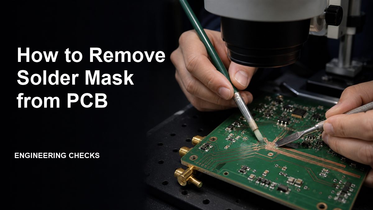
What Removing Solder Mask From a PCB Means
Removing solder mask means taking away the protective coating above the copper so the copper can be inspected, soldered, probed, or repaired. On most finished boards, the solder mask protects traces from oxidation, solder bridges, fingerprints, flux residue, and accidental contact.
In plain words, you are opening a small window in the protective layer. That window may be useful, but it also removes protection. After the work is finished, the exposed area should usually be tinned, cleaned, coated, or otherwise protected.
When You Should Remove Solder Mask
You should remove solder mask only when there is a clear job to do underneath it. Common reasons include trace repair, jumper wire attachment, test-point access, pad recovery, solder bridge investigation, or checking whether a copper trace is damaged.
For example, if a trace is broken between two pads, a small exposed copper area gives you a place to solder a repair wire. If a board has no accessible test point, exposing a short section of copper may allow a temporary measurement. The best reason is always specific and local, not cosmetic.
When You Should Not Remove Solder Mask
Do not remove solder mask just because a board looks dirty, because a trace is hard to see, or because a solder joint looks dull. Many board problems can be checked with inspection, continuity testing, cleaning, or X-ray/AOI before the protective coating is disturbed.
Do not remove mask from high-speed traces, impedance-controlled routes, fine-pitch BGA escape areas, flex bend zones, high-voltage creepage areas, or dense multilayer boards unless the repair method has been reviewed. A small scrape in the wrong place can create a bigger reliability problem than the original defect.
Tools You Can Use to Remove Solder Mask
The safest tool depends on board value, copper width, mask hardness, and how much area must be exposed. Mechanical tools give better local control. Chemical removers may be useful on some coatings, but they add contamination and material compatibility risk.
| Method | Best Use | Main Risk | Buyer or Engineer Note |
| Fiberglass pen | Small trace exposure and repair prep | Glass dust and over-abrasion | Use mask, cleaning, and magnification |
| Precision scraper | Opening a narrow copper area | Cutting trace edge | Use shallow angle and light pressure |
| Micro drill or burr | Controlled removal on larger areas | Pad lift and copper thinning | Only for experienced repair work |
| Chemical remover | Selected coating removal | Residue and material attack | Verify compatibility before use |
| Laser ablation | Production or precision rework | Heat and setup error | Best handled by qualified repair shop |
Step-by-Step: How to Remove Solder Mask Safely
Use a small, controlled process instead of trying to clear a large area at once.
Step 1: Confirm why the mask must be removed. Mark the exact copper area, not a general region.
Step 2: Secure the PCB on a stable bench. Use magnification and good lighting so you can see the trace edge.
Step 3: Clean the surface with suitable electronics cleaner or isopropyl alcohol, then let it dry.
Step 4: Use a fiberglass pen or precision scraper with light pressure. Work from the mask surface down toward the copper, not sideways into the trace.
Step 5: Stop as soon as bright copper is visible. Do not keep scraping to make the area look perfect.
Step 6: Remove dust and residue. If fiberglass is used, clean carefully because loose fibers can irritate skin and contaminate the board.
Step 7: Test continuity before soldering. A trace that was damaged during scraping should be repaired before the next step.
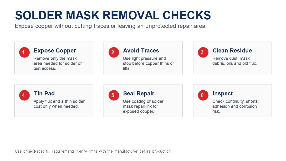
How to Avoid Cutting the Copper Trace
The easiest way to damage the board is to treat the solder mask like paint on a wall. PCB copper is thin, and a small trace can be cut or narrowed before you notice it.
Work with the tool almost flat to the board surface. Use repeated light passes instead of one hard scrape. If the copper trace is narrow, scrape across the mask edge slowly and stop when the copper appears. After exposure, use a multimeter to check continuity from one known pad to another.
How to Clean and Tin the Exposed Copper
After the mask is removed, the exposed copper should be cleaned before solder is applied. Flux works better on clean copper, and solder wetting tells you a lot about surface condition.
Apply a small amount of flux, heat the copper briefly, and add only enough solder to wet the exposed area. A thick solder mound can bridge nearby traces or create mechanical stress. If the exposed copper is only for testing, do not tin it unless the test method requires it.
How to Protect the Area After Repair
Bare copper should not stay exposed unless the design intentionally requires it. After repair, use solder mask repair ink, conformal coating, suitable epoxy, or controlled tinning depending on the electrical and environmental requirement.
If the board operates in humidity, vibration, outdoor equipment, industrial control, automotive electronics, or high-voltage environments, protection is not optional. The repair should be inspected again after coating because some coating materials can flow into connectors, switches, or test pads.
Removing Solder Mask for PCB Rework vs Manufacturing
Bench repair and factory manufacturing are different situations. In repair, the goal is to recover one board or create temporary access. In manufacturing, the goal is repeatability, controlled exposure, and documentation.
| Situation | Goal | Better Control Method | Risk to Check |
| One-board repair | Expose a trace or pad locally | Microscope, scraper, fiberglass pen | Trace cut, lifted pad, contamination |
| Prototype modification | Add jumper or test access | Documented rework instruction | Repeatability across samples |
| Production change | Change exposed copper pattern | Update Gerber and solder mask layer | Old files used by mistake |
| Quality investigation | Inspect hidden copper defect | Cross-section or lab analysis | Destroying evidence during scraping |
Common Mistakes That Damage the Board
The most common mistake is removing too much mask. A larger exposed copper area is harder to protect and easier to bridge with solder. Another mistake is scraping toward a pad edge, which can lift the pad or weaken the adhesive bond.
Other common mistakes include using a knife without magnification, using aggressive chemicals without compatibility checks, skipping continuity testing, soldering before cleaning dust, and leaving exposed copper unsealed after the repair.
Inspection Checklist After Solder Mask Removal
Inspection should be simple and strict. The board may look repaired but still fail later if copper is narrowed, residue remains, or the repair area is left open.
| Check | What to Look For | Why It Matters |
| Copper continuity | Stable resistance across the trace path | Confirms the trace was not cut |
| No shorts | No bridge to nearby copper | Prevents immediate electrical failure |
| Trace width | No visible thinning or gouge | Reduces current and reliability risk |
| Residue | No dust, fibers, old flux or chemical film | Reduces leakage and corrosion risk |
| Protection | Coating or solder coverage where needed | Prevents oxidation and handling damage |
What to Tell a PCB Supplier or Repair Partner
If the repair is connected to a prototype build, board redesign, or production issue, give the supplier enough context to judge the risk. Do not only say “remove solder mask here.” Explain why the area needs to be exposed and what function it serves.
Useful information includes Gerber files, board photos, copper layer location, trace width, copper weight, board finish, rework reason, quantity, operating environment, and whether the exposed area must be sealed after soldering.
How PCB Design Can Avoid Manual Solder Mask Removal
The best repair is the one you do not need later. Add test points, exposed pads, jumper pads, or optional solder bridges during PCB design if you know the board may need debugging or configuration.
If a trace may need current measurement, bring it to a pad. If a firmware or calibration process needs probing, add documented test points. For production, any intentional exposed copper should be defined in the solder mask layer rather than created manually after fabrication.
Internal Links for Related PCB Decisions
Solder mask removal often connects to copper, material, and board reliability decisions. For related engineering background, review how to choose PCB copper thickness, PCB thickness tolerance, FR4 substrate material, and heavy copper PCB design.
FAQs About Removing Solder Mask From PCB
Can I remove solder mask with a knife?
A knife can work on a low-value board, but it is easy to cut copper or lift a pad. A fiberglass pen or controlled scraper is usually safer.
Can I use sandpaper?
Fine abrasive can remove mask, but it is less controlled near small traces. It also creates dust that must be cleaned carefully.
Is chemical solder mask remover safe?
It depends on the board material, coating, component exposure, and cleaning process. Verify compatibility before using chemicals on a working PCB.
Should I remove solder mask before soldering a jumper wire?
Yes, if there is no pad available. Expose a small copper area, tin it lightly, solder the jumper, then protect the repair.
How do I know if I scraped too deep?
Check continuity and inspect the trace under magnification. A gouged, narrowed, lifted, or broken copper line means the repair needs correction.
Do I need to coat the exposed copper again?
Usually yes, especially for boards used in humid, dirty, high-voltage, or industrial environments.
Can solder mask removal damage impedance-controlled traces?
Yes. It can change local geometry and surface condition. Avoid scraping impedance-sensitive routes unless the repair is reviewed.
What files help a supplier review a solder mask issue?
Gerbers, photos, copper layer data, board finish, repair location, quantity, and the reason for exposure are the most useful starting points.
Can PCBTRY help review a solder mask repair or redesign?
Yes. Send board photos, Gerbers, copper details, and the repair goal to [email protected] for engineering review.
Send PCB Repair or Rework Requirements for Review
If your board needs solder mask removal, trace repair, exposed copper changes, or a production file update, send the Gerber files, photos, copper layer notes, quantity, and repair purpose to [email protected]. PCBTRY can review whether the issue should be handled as bench repair, prototype modification, or a design update before the next PCB build.



0 Comments