




How Does a PCB Work in Simple Terms?
A PCB works like a planned road system for electricity. The green board is not the part that thinks or powers the product by itself. It holds copper paths, called traces, and those traces connect components so power and signals can move in the right order.
In plain words, the PCB gives every electronic part a fixed place to sit and a controlled path to talk to other parts. A battery connector, voltage regulator, microcontroller, sensor, LED or connector can only do its job when the copper paths between them are correct.
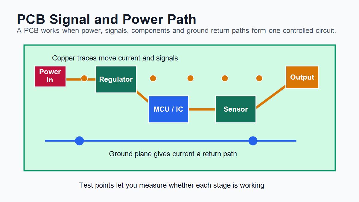
The easiest way to understand it is this: power enters the board, travels through copper, reaches the components, returns through ground, and signals move between parts to make the product respond. If one trace is broken, one part is rotated wrong, or the return path is poor, the whole circuit may stop working even if the components themselves are good.
What Parts of a PCB Carry Signals and Power?
The main working parts of a PCB are copper traces, pads, vias, planes, solder mask, silkscreen and mounted components. Beginners often look at the components first, but the copper network is what makes those components work together.
Power traces carry voltage and current. Signal traces carry information, such as a sensor reading, a clock signal or a control command. Ground planes give current a return path. Pads let components solder to the board. Vias move a connection from one layer to another.
| PCB part | What it does | Why it matters | What to check |
|---|---|---|---|
| Copper trace | Moves current or signal between points | Wrong width or route can cause voltage drop, noise or overheating | Trace width, spacing, current load and impedance needs |
| Pad | Gives a component lead or terminal a solderable landing area | Poor pad size can cause weak solder joints or assembly defects | Footprint, solder mask opening and component polarity |
| Via | Connects one copper layer to another | Bad via design can break signals or increase resistance | Drill size, annular ring, plating and via count |
| Ground plane | Provides a low-resistance return path | A poor ground path can create noise and unstable behavior | Continuity, return path, split planes and high-speed paths |
| Solder mask | Protects copper and reduces solder bridging | Incorrect openings can expose copper or block soldering | Clearance around pads, vias and fine-pitch parts |
| Silkscreen | Shows labels, polarity marks and reference designators | Bad marking can lead to wrong assembly or testing mistakes | Readable labels, polarity marks and no text on pads |
How Do Copper Traces Connect Components?
Copper traces work like wires printed on a flat board. Instead of hand-soldering loose wires between every part, the PCB manufacturer etches copper into planned paths. Those paths connect pins according to the circuit design.
For example, a sensor may send a signal to a microcontroller. The trace between the sensor output pin and the microcontroller input pin is the road that carries that signal. If that trace is cut, routed to the wrong pin, too narrow for the current, or placed too close to a noisy power trace, the circuit may behave incorrectly.
This is why PCB layout is not just drawing lines. The trace must fit the electrical job. A small logic signal can use a narrow trace. A motor current path needs more copper. A high-speed or impedance-controlled signal needs controlled geometry and a good return path. If you are learning layout, this related guide on how to make PCB layout explains placement and routing checks in more detail.
Why Do PCB Layers, Planes and Vias Matter?
PCB layers matter because one flat surface cannot always carry every connection cleanly. A simple board may use one or two copper layers. More complex boards use four, six or more layers so power, ground and signals can be separated and controlled.
A via is a small plated hole that lets a connection move from one layer to another. Think of it as a vertical elevator for electricity. If a trace cannot pass another trace on the same layer, a via can move it to a different layer and bring it back later.
Planes are large copper areas, often used for ground or power. A ground plane is important because current does not just leave a power source and disappear. It must return to the source. When the return path is short and stable, the board usually has less noise and more predictable behavior.
For manufacturing, layer count, via structure and stackup affect cost, drilling, plating, impedance and inspection. If a board needs controlled impedance, the trace width, copper thickness, dielectric thickness and reference plane must work together. For a deeper measurement view, see this pcbtry guide on how to measure PCB trace impedance.
How Do Components Use the PCB to Form a Circuit?
Components are the active and passive parts that make the circuit do useful work. The PCB gives them both mechanical support and electrical connections. A resistor limits current, a capacitor stores and filters charge, an IC processes signals, and a connector brings signals or power in and out of the board.
A single component rarely works alone. A voltage regulator may need input capacitors, output capacitors, a ground path and a copper area for heat. A microcontroller may need power pins, ground pins, clock components, programming pins and signal lines. The PCB ties these pieces together so they behave like one circuit instead of separate parts.
The common beginner mistake is to think the schematic and PCB are the same thing. The schematic says what should connect. The PCB layout decides how those connections physically happen. A correct schematic can still fail if the PCB footprint, routing, layer stack or assembly polarity is wrong. This is why designing a PCB board for a circuit needs both circuit logic and manufacturing review.
What Happens When Power First Enters a PCB?
When power first enters a PCB, it usually goes through protection, filtering and regulation before it reaches sensitive parts. The exact path depends on the product, but the logic is similar: protect the board, clean up the supply, create the right voltage, then distribute that voltage to the circuit.
Step 1: Power enters through a connector, battery terminal, USB port or another input. At this point, the board must handle the expected voltage, current and polarity.
Step 2: Protection parts may block reverse polarity, reduce surge damage, or protect against electrostatic discharge. These parts are especially important near external connectors.
Step 3: Filtering capacitors reduce noise and voltage dips. Without stable local power, ICs can reset, sensors can drift, and communication signals can become unreliable.
Step 4: A regulator creates the voltage that the circuit needs, such as 5 V, 3.3 V or another rail. The regulator also needs the right copper area and component placement to manage heat and stability.
Step 5: Power reaches the loads, and current returns through ground. If the return path is weak, long or interrupted, the board may work on the bench but fail under load.
How Do Test Points Help You Check a PCB?
Test points are small places on the PCB where you can measure voltage, signals or continuity. They help engineers and technicians check whether each stage of the board is working.
A test point is useful because a PCB problem is often hidden. You cannot see current moving through copper. By placing test points at power rails, ground, reset lines, communication lines and key outputs, you can divide the circuit into stages and find where the problem begins.
| Test point location | What it helps verify | Typical problem it can reveal |
|---|---|---|
| Power input | Correct incoming voltage and polarity | Wrong adapter, reversed input, loose connector |
| Regulator output | Stable rail voltage | Wrong component, shorted rail, overheating regulator |
| Ground | Good reference and continuity | Broken return path or poor solder joint |
| Reset or enable pin | Whether an IC is allowed to start | Device held in reset or missing pull-up/pull-down |
| Signal output | Whether a circuit block is producing the expected response | Bad sensor, wrong routing, wrong firmware or assembly error |
For prototype or production review, test points should be planned before manufacturing. Adding them after the board is built is harder and may require rework.
What PCB Design Problems Stop a Board from Working?
A PCB usually fails because one part of the connection chain is wrong: wrong connection, weak solder joint, poor power path, bad return path, wrong footprint, incorrect component orientation or manufacturing defect.
The important teaching point is that a PCB problem is not always a “bad board.” Sometimes the bare PCB is correct but the assembly is wrong. Sometimes the schematic is correct but the layout is weak. Sometimes the layout is correct but the manufacturing files are incomplete.
| Problem | What it means in simple terms | How it affects the board | Before manufacturing check |
|---|---|---|---|
| Open trace | The copper path is broken | Signal or power cannot reach the next part | Gerber inspection and electrical net check |
| Short circuit | Two nets touch when they should not | Overcurrent, heat, damaged parts or no startup | Spacing, solder mask and DRC review |
| Wrong footprint | The pad pattern does not match the component | Component cannot solder correctly or pins connect wrong | Footprint-to-datasheet comparison |
| Poor ground return | Current has a bad path back to the source | Noise, resets, unstable readings or EMI issues | Plane review and high-current path review |
| Undersized trace | The copper is too narrow for the current | Voltage drop or overheating | Trace width and copper thickness check |
| Missing polarity mark | The board does not clearly show orientation | Diodes, LEDs, ICs or capacitors may be assembled backwards | Silkscreen and assembly drawing review |
What Manufacturing Checks Help a PCB Work Reliably?
Manufacturing checks help confirm that the design can become a real board without avoidable defects. A PCB does not work just because the idea is correct. It works when the Gerber files, drill files, stackup, copper rules, solder mask, surface finish and inspection steps all match the design intent.
Before production, a manufacturer should review whether the board can be fabricated within process limits. This includes minimum trace width and spacing, hole size, annular ring, copper-to-edge clearance, solder mask bridges, board thickness, material choice and surface finish. If the board has high-speed, high-current, HDI, flex or controlled impedance requirements, the review must be stricter.
For a broader process view, this pcbtry guide on how to manufacture PCB board explains Gerber review, drilling, plating and final checks from a factory perspective.
| Check | Why it matters | What to send or confirm |
|---|---|---|
| Gerber and drill review | Confirms copper, solder mask, silkscreen and hole data are complete | Gerber files, Excellon drill file and board outline |
| Stackup review | Confirms layers, thickness and copper structure | Layer count, finished thickness and copper weight |
| DFM check | Finds manufacturability risks before production | Minimum trace/space, hole size, annular ring and clearance limits |
| Electrical test | Checks for opens and shorts on the bare board | Netlist if available, test requirement and acceptance expectation |
| Assembly file check | Prevents placement and polarity mistakes | BOM, CPL, assembly drawing and polarity notes if assembly is required |
PCB Working Checklist Before Manufacturing
Use this checklist before sending a PCB to fabrication. It is written for beginners, but it also helps buyers and engineers avoid common handoff mistakes.
- Confirm the schematic connections are final and match the intended circuit function.
- Check that every power rail has a clear path from input to load and back to ground.
- Review trace width for current, not only for routing convenience.
- Check high-speed or impedance-sensitive traces against the stackup and reference plane.
- Confirm every component footprint against the datasheet and package option.
- Verify polarity marks for LEDs, diodes, electrolytic capacitors, connectors and IC pin 1.
- Place useful test points on input voltage, regulated rails, ground and key signals.
- Run design rule checks and inspect Gerber output, not only the layout file.
- Send complete Gerber, drill, board outline, stackup and specification notes to the PCB manufacturer.
- For assembly, also send BOM, CPL, assembly drawing, substitution rules and testing requirements.
FAQ About How a PCB Works
Does a PCB work without components?
A bare PCB can carry connections, but it usually cannot perform the final electronic function without components. The copper paths are like roads; the components are the devices that use those roads.
What makes electricity move on a PCB?
Electricity moves when there is a voltage source and a complete circuit path. Current travels through copper traces, components and the ground return path.
Why are PCB traces copper?
Copper conducts electricity well, can be etched into precise patterns, and can be plated for holes and surface finishes. That makes it practical for PCB manufacturing.
What is the difference between a trace and a wire?
A trace is a flat copper path made on the PCB. A wire is a separate conductor. Both can connect points, but traces are built into the board and can be manufactured repeatedly.
Why does ground matter on a PCB?
Ground gives current a return path and a reference point for signals. Poor ground routing can cause noise, resets, measurement errors and unstable operation.
Can a PCB fail even if the schematic is correct?
Yes. A correct schematic can still fail because of poor layout, wrong footprints, weak return paths, manufacturing defects or assembly mistakes.
How do vias help a PCB work?
Vias connect copper between layers. They let a signal, power rail or ground connection move vertically through the board when one layer is not enough.
What should I check before ordering a PCB?
Check Gerber files, drill files, board outline, stackup, copper weight, minimum trace/space, hole sizes, surface finish, test requirements and assembly files if components will be mounted.
How can I tell whether a PCB is working?
Measure power input, regulator outputs, ground continuity and key signals at test points. If one stage is wrong, debug that stage before assuming every part of the board is bad.
Do all PCBs need testing?
For production, bare board electrical testing is strongly recommended because it can catch opens and shorts before assembly. Functional testing is also useful when the board is assembled.
Need a PCB Manufacturing Review Before Production?
If your PCB design is ready for fabrication, send your Gerber files, drill file, board thickness, copper weight, material requirement, surface finish and quantity to [email protected]. If the board also needs assembly, include BOM, CPL, assembly drawing and testing requirements so the engineering team can review manufacturability, quote risks and production checks before you place the order.



0 Comments