




How to Tell if PCB Is Damaged in Simple Terms
You can tell if a PCB is damaged by checking for visible damage first, then using power-off tests, then using careful power-on measurements only when the board is safe to energize. A damaged PCB may show burn marks, cracked laminate, lifted pads, broken traces, corrosion, shorted power rails, hot components, unstable voltage or intermittent operation.
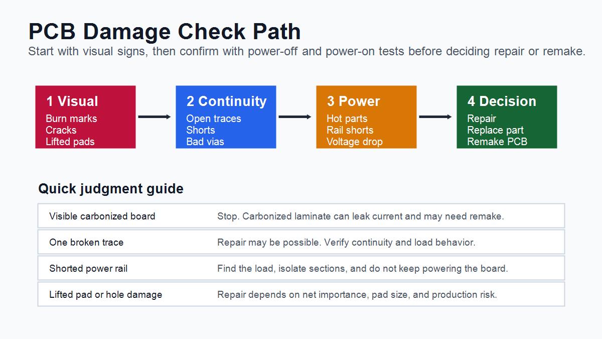
The important point is this: a PCB can look clean and still be electrically damaged. It can also look ugly but still have one repairable broken trace. That is why you should not judge by appearance alone. You need a simple inspection path: look, measure continuity, check power rails, then decide whether repair, component replacement or PCB remake is the safer choice.
Start with Visual Signs of PCB Damage
Visual inspection is the safest first step because it does not require powering the board. Use good light and magnification. Look for burned areas, darkened laminate, cracked board edges, lifted pads, missing copper, broken traces, swollen capacitors, corrosion, solder bridges and loose connectors.
Do not only look at the top side. Many failures appear on the bottom side, around connector pins, high-current traces, relays, hot components or areas near liquid exposure. If the board has a shield, enclosure or conformal coating, inspect the places where heat and moisture can hide.
| Visible sign | What it means in plain language | Risk level | Next check |
|---|---|---|---|
| Burned or carbonized laminate | The board material has overheated and may conduct leakage current | High | Do not power until the damaged area is isolated |
| Lifted pad | The copper pad has separated from the board | Medium to high | Check whether the connected net is still continuous |
| Broken trace | The copper road between two points is cut | Medium | Use continuity mode to confirm the open path |
| Corrosion | Moisture or chemicals may have attacked copper or component leads | Medium to high | Inspect under components and test nearby nets |
| Solder bridge | Solder connects two points that should stay separate | High | Check for shorts before applying power |
| Cracked board edge | The laminate and copper layers may be mechanically damaged | Medium | Check traces and vias crossing the cracked area |
Use a Multimeter Before You Apply Power
A multimeter helps confirm whether a suspected PCB damage point is only cosmetic or actually electrical. Before applying power, use continuity and resistance checks. This is safer than powering a board that may have a short.
Step 1: Check continuity across suspected broken traces. If the meter does not beep where a copper path should connect, the trace, via or solder joint may be open.
Step 2: Check for shorts between power and ground. If a power rail reads near zero ohms to ground, stop and find the short before powering the board.
Step 3: Compare similar circuits if the board has repeated channels. A different resistance reading on one channel can reveal a damaged component or damaged copper path.
Step 4: Check connector pins and mechanical stress points. Connectors often crack solder joints or pull pads loose because they receive force from cables.
Check Power Rails Carefully
Power rail checks tell you whether the board can distribute voltage safely. A damaged PCB often fails at the power input, regulator output, ground return path or high-current load path.
If the board passed basic power-off checks, apply current-limited power when possible. Start with a low current limit and watch for abnormal current draw, voltage collapse, smoke, smell or sudden heating. If current jumps immediately, remove power and return to short-circuit diagnosis.
Measure the input voltage, regulator output, ground continuity and key IC supply pins. A board may receive correct input voltage but still fail because a regulator, via, connector, fuse, trace or solder joint interrupts the path. If you need a broader diagnostic sequence, QFPCB has related PCBA testing content, but for pcbtry this article focuses on bare PCB and manufacturing review boundaries.
Look for Heat, Smell and Intermittent Behavior
Heat and smell are warning signs, but they must be handled carefully. A hot component may be the failed part, or it may only be heating because another damaged trace, shorted capacitor or wrong supply path is forcing current through it.
If the board works sometimes and fails when touched, moved or warmed, suspect cracked solder joints, broken traces, damaged vias or connector stress. Intermittent PCB damage is often harder to find than a fully burned board because the connection may open only under vibration, heat or bending.
Do not keep powering a board to “see what happens.” Repeated power cycling can turn a repairable problem into burned laminate or damaged components.
How to Tell if a PCB Trace Is Damaged
A PCB trace is damaged when the copper path is broken, burned, corroded, lifted or shorted to another net. In simple terms, the electrical road is no longer doing the job it was designed to do.
Use continuity mode between both ends of the trace. If the path should connect but does not, the trace may be open. If the trace connects to a nearby net that should be separate, there may be a solder bridge, copper smear, conductive contamination or carbonized board material.
For repair decisions, trace location matters. A low-current indicator trace may be repairable with a jumper wire. A high-current, high-frequency, impedance-controlled or safety-critical trace may need redesign or remanufacture. For trace repair details, see pcbtry’s guide on how to repair a PCB trace.
How to Tell if Pads, Vias or Plated Holes Are Damaged
Pads, vias and plated holes are common failure points because they connect components and layers. A pad can lift during rework, a via can crack from mechanical stress, and a plated hole can fail if drilling, plating or repeated heating damages the barrel.
A damaged pad may no longer hold solder well or may disconnect from its trace. A damaged via may look normal from the outside but fail continuity between layers. A plated through hole may lose connection on one side while still appearing soldered.
Check continuity from the component pad to the next known point on the same net. For vias, check both sides of the board or another connected pad. If the board uses fine traces, dense vias or multilayer routing, repair becomes less predictable. This is where a manufacturing review helps decide whether the original Gerber and drill design need improvement.
When Is PCB Damage Repairable?
PCB damage is usually repairable when the affected net is simple, accessible, low-current and not safety-critical. A broken low-speed trace, lifted test pad, damaged solder mask area or small corrosion spot may be repairable after cleaning and verification.
Repair becomes risky when the board has carbonized laminate, internal layer damage, high-current copper damage, controlled impedance traces, repeated via failures, connector force damage or unknown moisture contamination. In those cases, the board may work after repair but fail again under load, vibration or temperature change.
| Damage type | Often repairable? | Why | Best next action |
|---|---|---|---|
| Single broken low-current trace | Often yes | The path can sometimes be bridged and tested | Repair, inspect and load test |
| Lifted non-critical pad | Sometimes | Depends on mechanical stress and remaining copper | Repair only if the connection can be anchored |
| Burned carbonized board | Usually risky | Carbonized material can leak current | Consider redesign or remake |
| Internal layer crack | Usually no | The failure path is hidden and hard to verify | Remake or redesign |
| Corrosion under ICs | Risky | Damage may continue under components | Clean, inspect, then decide replacement |
When Should You Stop Testing a Damaged PCB?
You should stop testing when continued power or heat can make the board more dangerous or less diagnosable. Stop if you see smoke, smell burning, detect a power-to-ground short, find carbonized laminate, see current climbing abnormally, or notice a component heating quickly without a clear reason.
Stopping is not giving up. It protects the board, the components, the test equipment and the person doing the work. A controlled pause lets you isolate loads, remove suspect components, compare nets, review schematics and decide whether the board should be repaired or remade.
Manufacturing Problems That Can Look Like PCB Damage
Some apparent PCB damage actually comes from manufacturing or assembly problems. For example, poor solder mask clearance can look like exposed copper damage. Weak via plating can create intermittent opens. Wrong footprint design can cause pad lifting during assembly or rework.
Before blaming handling or use, check whether the same failure repeats on multiple boards. Repeated failures often point to design, fabrication or assembly conditions rather than one isolated accident.
Useful manufacturing checks include Gerber inspection, drill review, annular ring review, solder mask clearance, electrical testing and stackup confirmation. For a factory-side process view, see how to manufacture PCB board.
PCB Damage Checklist Before Repair or Remake
Use this checklist before deciding whether to repair the PCB, replace a component or remake the board.
- Photograph the damaged area before cleaning or repair.
- Check both sides of the board under good light and magnification.
- Mark burned areas, lifted pads, broken traces, corrosion and cracked edges.
- Use continuity mode to test suspected broken traces and vias.
- Check resistance between each power rail and ground before applying power.
- Use current-limited power if the board must be energized.
- Measure input voltage, regulator outputs and key component supply pins.
- Stop if current rises abnormally, a component heats quickly or the board smells burned.
- Decide whether the damaged net is low-risk and accessible enough for repair.
- For production boards, review Gerber, drill, stackup and assembly process before remaking.
FAQ About How to Tell if PCB Is Damaged
Can a PCB be damaged without visible burn marks?
Yes. A PCB can have cracked vias, broken internal traces, corrosion under components, bad solder joints or shorted power rails without obvious burn marks.
Is a dark spot on a PCB always serious?
Not always, but carbonized or burned laminate is serious because it may leak current. Inspect the area and avoid powering the board until the risk is understood.
How do I check a PCB for a short?
With power removed, use resistance or continuity mode between power rails and ground. If a rail reads very low resistance, isolate loads before applying power.
Can a broken PCB trace be repaired?
Sometimes. A simple low-current trace can often be bridged, but high-current, high-speed or safety-critical traces need stricter review.
What does a lifted PCB pad mean?
A lifted pad means copper has separated from the board surface. The electrical connection may be broken, and the component may no longer have a strong solder joint.
Why does my PCB work only when I press on it?
That often suggests an intermittent connection, cracked solder joint, damaged via, loose connector or broken trace that reconnects under pressure.
Should I power a damaged PCB to test it?
Only after power-off checks show no obvious short or severe burn risk. Use current-limited power when possible and stop immediately if current or heat looks abnormal.
Can water damage a PCB permanently?
Yes. Moisture can cause corrosion, conductive residue and hidden damage under components. Cleaning may help, but the board still needs inspection and testing.
How do I know whether to repair or remake a PCB?
Repair is more reasonable for accessible, low-risk damage. Remake is safer for carbonized laminate, internal layer damage, repeated failures or production boards with design/process issues.
What files help a manufacturer review PCB damage risk?
Gerber files, drill files, stackup notes, board photos, failure location, current path information, BOM and assembly notes help the manufacturer judge whether design or production changes are needed.
Need PCB Damage or Manufacturing Review?
If your PCB shows burn marks, broken traces, lifted pads, corrosion or repeated electrical failure, send board photos, Gerber files, drill files, stackup notes, copper weight, surface finish and failure details to [email protected]. PCBTRY can review whether the issue looks repairable, design-related, fabrication-related or better solved by remaking the PCB with corrected manufacturing checks.



0 Comments