




How Wide Should PCB Traces Be for Different Net Types?
PCB traces should be wide enough to meet the electrical requirement and comfortably manufacturable, but there is no single correct width for every net. For an ordinary low-current signal on a standard board, a designer may start with a conservative fabrication-friendly width such as 8-12 mil (0.20-0.30 mm). A power trace must instead be sized from current, copper thickness, allowable temperature rise, layer position, length, and voltage drop. A high-speed or RF trace may have its width fixed by a controlled-impedance calculation rather than by current.
The useful question is therefore not, “What default width does my CAD tool use?” It is, “Which requirement controls this net?” Use the following table as the first decision.
| Net type | What usually controls width | Practical starting action |
|---|---|---|
| Low-current, low-speed signal | Fabrication margin, routing density, pad pitch | Choose a comfortable width above the fabricator’s minimum unless a tight escape requires less |
| DC power or ground branch | Continuous current, copper thickness, temperature rise, length, voltage drop | Calculate the required copper cross-section, then check the entire current path |
| High-current rail | Heat, voltage drop, connector/pad/via bottlenecks, available copper area | Evaluate pours, planes, heavier copper, multiple layers, or a bus structure |
| High-speed digital or RF signal | Target impedance and actual stackup geometry | Obtain the stackup and solve the width with the fabricator or a field solver |
| High-voltage net | Clearance, creepage, insulation system, contamination environment | Set spacing first; do not assume a wider trace solves voltage-isolation risk |
This distinction prevents the most common mistake: applying a current calculator to every signal or applying one “standard” signal width to a power rail.
Why the Fabricator’s Minimum Width Is Not Your Design Target
A fabricator’s minimum trace width tells you what the process can produce under specified conditions. It does not tell you how much current the trace can carry, how much voltage it will lose, or whether it will meet an impedance target.
For example, a board house may list 4 mil or 6 mil as a standard capability. That means a trace of that width may be manufacturable with the associated copper thickness, spacing, layer count, and tolerance. It does not make 4 mil the best default for every low-current signal. Staying away from the process limit where space allows can improve etching margin and reduce the chance that local copper-width variation becomes important.
There are valid reasons to use a narrow trace: escaping a fine-pitch BGA, passing between pads, meeting an impedance geometry, or fitting a dense routing channel. Treat these as controlled exceptions. Define a short neck width and maximum neck length instead of silently letting an entire net inherit the minimum rule.
If you are new to the geometry, start with what a PCB trace is and how it connects pads and vias, then return to the electrical sizing process below.
Which Inputs Actually Determine Current-Carrying Width?
Current-carrying width cannot be calculated from amperes alone. At minimum, record the continuous current, copper thickness, allowed temperature rise, layer location, and trace length. Peak current, ambient temperature, nearby heat sources, airflow, and adjacent copper can also change the answer.
Start by naming the kind of current instead of copying the largest number from a datasheet. A trace that carries 2 A continuously has a different thermal problem from one that carries 8 A for 10 milliseconds every few seconds.
| Current description | What it means | What the width check must answer |
|---|---|---|
| Continuous current | The current can remain for long enough to approach thermal equilibrium | Can the trace stay within its allowed temperature rise and voltage-drop budget? |
| RMS current | The heating-equivalent value of a changing current | Is the RMS value based on the real waveform and duty cycle? |
| Peak or pulse current | A short event above the normal current | Is the pulse energy, repetition rate and permitted voltage dip acceptable? |
| Inrush current | A startup surge, often caused by motors, lamps or charging capacitors | Will the path, connector and protection devices tolerate startup without excessive sag? |
| Fault current | An abnormal current before a fuse or protection circuit clears | Must the copper survive until protection operates, or is the trace intentionally part of protection? |
| Input | Where to get it | What goes wrong if it is guessed |
|---|---|---|
| Continuous or RMS current | Load analysis, power budget, regulator or motor data | A peak-only or typical-only value can understate heating |
| Peak/inrush current and duration | Load transient, capacitor charge, motor startup, fuse profile | A trace may survive thermally but create a damaging voltage dip |
| Finished copper thickness | Stackup and fabrication specification | Nominal foil weight may not equal the final local copper thickness |
| Allowed temperature rise | Reliability and thermal budget | An arbitrary 10 C or 20 C assumption may conflict with the enclosure or nearby parts |
| Layer position | PCB stackup | Outer- and inner-layer heat spreading are not interchangeable |
| Length | PCB layout | A thermally acceptable trace may still have excessive resistance and voltage drop |
| Impedance target | Interface specification and stackup | Widening a high-speed trace can move it away from its required impedance |
Standards and calculators are engineering references, not guarantees for every board. IPC-2152 describes the relationship among current, conductor size, and acceptable temperature rise, while many web calculators use curve-fit equations derived from IPC-2221. The official IPC revision table currently identifies IPC-2152 as no longer maintained, so record the method and assumptions used instead of writing only “per IPC” in a design note.
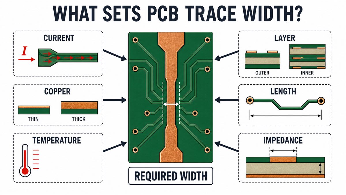
How the PCB Trace Width Formula Works
The common PCB trace-width formula first estimates the copper cross-sectional area needed for a current and temperature rise. It then converts that area into a width by dividing by copper thickness. In plain language, the formula is asking: “How much copper must this current pass through if I accept this amount of heating?”
Many IPC-2221-based calculators use the curve-fit equation:
I = k × ΔT0.44 × A0.725
Here, I is current in amperes, ΔT is the allowed conductor temperature rise in degrees Celsius, and A is copper cross-sectional area in square mils. Common calculator implementations use k = 0.048 for an external conductor and k = 0.024 for an internal conductor. After solving for area, use width = area / copper thickness, with area and thickness expressed in compatible units.
| Variable | Meaning | Beginner check |
|---|---|---|
| I | Current used for the thermal calculation | Use continuous or correctly calculated RMS current, not an unexplained peak |
| ΔT | Allowed rise above the local ambient temperature | A 10 C input is an assumption, not a universal safety limit |
| A | Copper cross-sectional area | This is thickness multiplied by width, not board surface area |
| k | Curve-fit constant for the conductor location | Confirm whether the calculator is treating the trace as internal or external |
Example: if a calculation says the required copper area is 60 mil2, nominal 1 oz copper at about 1.37 mil thick gives 60 / 1.37 = 43.8 mil of width. Nominal 2 oz copper at about 2.74 mil gives 60 / 2.74 = 21.9 mil. This example teaches the area-to-width conversion; it does not prove that either width is correct until current, temperature rise, layer, voltage drop and the full path have been checked.
Use the equation as a documented starting point, not as a warranty. The IPC-2221 curve fit simplifies the thermal environment. IPC-2152 adds broader empirical context, but the official IPC revision table marks IPC-2152 as no longer maintained. For a critical rail, preserve the inputs, compare methods where appropriate, and verify the assembled board under realistic load and cooling.
How Copper Weight and Layer Position Change the Result
Wider copper and thicker copper both increase the conductor’s cross-sectional area. More area lowers resistance, which reduces I2R heating and voltage drop for the same current and length. This is why 2 oz copper can carry the same current in less width than 1 oz copper, although heavier copper also changes etching, spacing, pad geometry, and cost.
Do not treat “1 oz” as a precise finished thickness at every point. It is a nominal copper-weight description. Base foil, plating, etching tolerance, and whether the feature is on an outer or inner layer affect the finished geometry. For a detailed selection path, see the PCB copper thickness guide.
| Nominal copper weight | Approximate thickness | How to use the value |
|---|---|---|
| 0.5 oz | 17 µm / 0.68 mil | Use only as an initial nominal value; confirm finished copper where it matters |
| 1 oz | 35 µm / 1.37 mil | Common starting construction, but plating and etching still affect local geometry |
| 2 oz | 70 µm / 2.74 mil | Reduces width for the same area, with manufacturing and spacing tradeoffs |
| 3 oz | 105 µm / 4.11 mil | Requires early confirmation of etching, spacing, pads and stackup |
| 4 oz | 140 µm / 5.48 mil | Treat as a deliberate heavy-copper construction, not a late layout change |
Layer position matters because the conductor exchanges heat with its surroundings differently. A simple IPC-2221 calculator often returns separate internal and external widths. More detailed thermal evaluation may also consider nearby planes, board thickness, adjacent conductors, airflow, components, and the enclosure. This is why the rule “make an inner trace exactly twice as wide” is only a rough starting heuristic, not a general law.
How PCB Material Changes Trace-Width Decisions
The copper still carries the current, but the board material changes how heat spreads, how the circuit bends, and what geometry can be manufactured reliably. Material is therefore a boundary condition for the trace-width decision, not a magic multiplier that automatically makes a trace safe.
| Board construction | What changes | What the designer should check |
|---|---|---|
| FR-4 rigid PCB | Common laminate with many established fabrication options | Stackup, finished copper, local ambient, planes, enclosure and fabrication tolerance |
| Flexible PCB | Thin polyimide construction bends and has different heat-spreading and mechanical constraints | Current and temperature plus bend radius, trace direction, copper type, repeated flexing and neck transitions |
| Metal-core PCB | A metal base can improve heat removal from selected structures | Actual dielectric path, copper geometry and thermal stack; do not automatically narrow the trace because a metal core exists |
| Ceramic PCB | High thermal conductivity and different conductor/manufacturing systems may be available | Substrate, metallization thickness, conductor process, attachment method and supplier-specific design rules |
For flex, metal-core or ceramic designs, ask the manufacturer for the proposed construction before freezing width. A calculator configured for a conventional external FR-4 trace may not represent the actual thermal and manufacturing environment.
How to Size a Power Trace Step by Step
Use a repeatable sequence so that a calculator result does not become an unexplained CAD number.
- Define the worst credible current. Separate continuous/RMS current from short transients. Record duration and duty cycle for pulses.
- Choose the copper construction. Record nominal and finished copper expectations, layer, and whether plating contributes to the feature.
- Set a temperature-rise budget. Base it on ambient temperature, enclosure cooling, adjacent components, laminate limits, and reliability needs.
- Calculate an initial width. Use a documented IPC chart, calculator, or validated thermal model. Save the method and all inputs.
- Check resistance and voltage drop. Use the actual routed length, not a guessed straight-line length.
- Inspect every bottleneck. Check pad exits, neck-downs, vias, plane slots, connector contacts, fuses, shunts, and return paths.
- Apply margin and manufacturing rules. Round to a practical width, define net classes, and confirm unusual copper geometry with the fabricator.
Example: suppose an outer-layer trace carries 2 A continuously on nominal 1 oz copper and the design allows a 10 C rise. A common IPC-2221 curve-fit calculator gives an initial result of about 31 mil (0.79 mm). That number is not a universal recommendation. Change the allowed rise, copper thickness, layer, environment, or calculation method and the result changes. A designer might round upward after checking available space, but must still calculate voltage drop and examine the rest of the path.
For a critical or high-volume product, validate the assumption with thermal measurement or simulation under realistic load and cooling. A calculator estimates a conductor; a test validates the assembled system.
When Voltage Drop Sets a Wider Limit Than Temperature
A trace can stay below its temperature-rise limit and still be too resistive for the circuit. This is common in low-voltage rails, remote sensors, LEDs, motors, and processors with tight supply tolerance.
The logic is simple: R = ρL/A, so copper resistance rises with length and falls as cross-sectional area increases. Vdrop = I × R, and the heat produced in the conductor is P = I2R. A long, narrow trace therefore loses more voltage and produces more heat than a short, wide trace carrying the same current.
If a 5 V rail can tolerate only 50 mV of PCB drop, the allowed end-to-end resistance at 2 A is 25 milliohms. That resistance budget includes the outgoing trace, return path, vias, connector contacts, protection devices, and other series elements, not just one visible copper segment. Symptoms of excessive drop can include regulator undervoltage, dim LEDs, weak motor torque, reset events or a sensor reading that changes with load.
Use the thermal calculation first, then calculate the routed resistance. If the predicted drop exceeds the power-integrity budget, widen or shorten the path, use more copper, improve the return, split current across appropriate layers, or change the power-distribution architecture. The stricter result controls.
When Impedance Controls Width Instead of Current
For a controlled-impedance signal, width is part of a transmission-line geometry. The target impedance depends on trace width and thickness, dielectric height and permittivity, reference-plane position, solder mask, copper roughness, and whether the structure is a microstrip, stripline, or differential pair.
A USB, Ethernet, RF, or other fast-edge net may carry very little DC current, yet its width cannot be chosen as an ordinary low-current signal. Obtain the proposed stackup first, solve the geometry, and let the fabricator adjust the production artwork within an agreed process if impedance compensation is required.
Do not “make it wider for safety” after the impedance calculation. That can lower impedance and create reflections. Also do not measure a fabricated impedance trace with a basic multimeter; controlled impedance is normally evaluated with methods such as TDR and, where appropriate, a test coupon. The PCB trace impedance measurement guide explains that workflow.
Where a Wide Trace Still Fails: Necks, Pads, Vias and Connectors
The current path is only as robust as its limiting section. A 3 mm copper pour does not help if all current must pass through one narrow pad exit, a small via, a slotted plane connection, or an undersized connector contact.
| Bottleneck | What to inspect | Why the main trace width is not enough |
|---|---|---|
| Pad neck-down | Minimum width, length, copper thickness, heat from the component | Local resistance and current density can be much higher than in the wide trace |
| Via transition | Finished hole, plating thickness, count, spacing, thermal environment | There is no reliable universal “amps per via” value |
| Connector pin | Contact rating, temperature rise, pin sharing, mating resistance | The connector may limit current before the PCB copper does |
| Thermal relief | Spoke count and width, soldering needs, actual current | Narrow spokes intentionally restrict copper connection |
| Plane slot or split | Available cross-section and return-current detour | A large plane can be narrowed by cutouts and antipads |
| Current-sense element | Kelvin routing, pad geometry, shunt power and tolerance | Functional measurement geometry may conflict with bulk-current routing |
A thermal relief connects a pad to a plane through narrow copper spokes. The spokes reduce heat flow into the plane so the pad can reach soldering temperature more easily. That same feature also reduces the electrical cross-section. For a low-current component this may be harmless; for a high-current terminal, shunt, connector or power device, the spokes can become the hottest part of the path. Check spoke width and count against current, but also check assembly needs before changing the pad to a solid plane connection. The correct answer balances current capacity with reliable soldering.
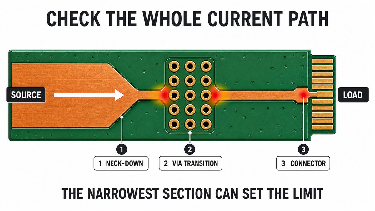
When a layer change is unavoidable, define the via structure with the board fabricator. Hole size, finished copper, via count, spacing, plane connection, current sharing, and thermal environment all matter. See how PCB vias are drilled and plated before treating a via as an ideal zero-resistance connection.
When to Use Copper Pours, Planes or Heavier Copper
A wider routed trace is not always the most practical way to carry more current. Use copper pours when an irregular area can provide a low-resistance path around components. Use planes when many loads need distributed power or ground and the stackup supports a continuous return structure. Consider heavier copper when the current and thermal requirement applies broadly enough to justify the manufacturing tradeoffs.
| Option | Best fit | Design caution |
|---|---|---|
| Wider trace | Defined point-to-point rail with available routing space | Check neck-downs and return path |
| Copper pour | Irregular local power area or thermal spreading | Check islands, slots, thermal reliefs and minimum necks |
| Power/ground plane | Distributed current and low-inductance return structure | Do not cut critical return paths with splits or antipads |
| Heavier copper | Many high-current features or demanding thermal design | Confirm spacing, etching, hole/pad geometry, stackup and cost |
| Multiple layers in parallel | High current where one layer lacks area | Provide enough transitions and verify current sharing |
For very high current, conventional PCB copper may no longer be the right architecture. Busbars, embedded copper structures, metal-backed solutions, or a different interconnect may be more appropriate. That decision should be made from system current, temperature, weight, volume, assembly, and service requirements rather than from trace width alone.
How Wide Should PCB Traces Be for Common Applications?
Application examples are useful only when they identify the controlling constraint. The table below gives a starting decision, not a list of guaranteed widths to copy into every board.
| Application | What usually controls the decision | Practical design action |
|---|---|---|
| GPIO and slow logic | Fabrication margin, density and pad pitch | Use a comfortable signal width above the process minimum where space allows |
| I2C, SPI or UART | Edge rate, route length, return path and coupling | Start with a normal signal rule, then add signal-integrity constraints when the interface requires them |
| MCU or sensor power | Current, transient demand and allowed supply drop | Check both steady current and local decoupling path |
| LED string or lighting board | Current, long route drop and thermal environment | Calculate the full loop and verify brightness or regulation at the far end |
| Motor or solenoid path | Continuous current, startup/stall current and switching loop | Separate operating, startup and fault conditions; inspect connectors and return copper |
| Battery input | Maximum load, inrush, protection clearing and connector rating | Check the path from connector through protection to load and back |
| MOSFET switching path | RMS/peak current, loop inductance, heat and pad necks | Use short, broad current loops and verify the package-pad connection |
| USB, Ethernet or RF | Controlled impedance and production stackup | Let the impedance geometry set width; current sizing is usually secondary |
| High-voltage circuit | Clearance, creepage and insulation coordination | Design spacing from the applicable safety conditions; width alone does not provide isolation |
| Flex, metal-core or ceramic board | Construction-specific thermal, mechanical and fabrication limits | Obtain the supplier’s stackup and rules before final width selection |
What Trace-Width Mistakes Cause Heat, Drop or Fabrication Risk?
| Mistake | Likely consequence | Better check |
|---|---|---|
| Using the CAD default for every net | Power rails too narrow or dense areas unnecessarily wide | Create net classes by electrical function |
| Entering typical current instead of worst credible continuous current | Unexpected heat and voltage sag | Review load, tolerance, fault and startup conditions |
| Copying a current table without its copper and temperature assumptions | False confidence in an inapplicable width | Record all calculation inputs and method |
| Ignoring trace length | Rail arrives below required voltage | Calculate end-to-end resistance and drop |
| Widening a controlled-impedance net | Impedance error and reflections | Use the actual stackup and impedance solution |
| Checking only the widest visible copper | Hot neck, via or connector failure | Audit the complete source-load-return path |
| Designing all geometry at the board house minimum | Higher process sensitivity and avoidable cost/yield pressure | Use minimum geometry only where routing requires it |
| Assuming solder mask removal alone creates a known current rating | Uncontrolled plating/solder thickness and assembly variability | Specify and validate the intended copper/current solution |
How to Put Trace Widths into CAD Rules and a DFM Package
A calculation becomes useful only after it is translated into enforceable design rules. Create net classes for ordinary signals, sensitive analog nets, controlled-impedance signals, low-current power, and high-current power. For each class, define nominal width, allowed neck width, neck-length limit, clearance, preferred layer, and via-transition rule where needed.
Before releasing fabrication data, include the information the manufacturer needs to interpret the geometry:
- Gerber or ODB++/IPC-2581 data, NC drill files, board outline, and fabrication drawing;
- layer stackup, material family, finished copper expectations, and finished board thickness;
- controlled-impedance targets, tolerance, reference layers, and coupon requirement;
- high-current net names, continuous/peak current, temperature assumptions, and unusual copper features;
- minimum trace/space exceptions, intentional neck-downs, and any heavy-copper requirement;
- electrical test and acceptance requirements.
Also identify any flex zone, metal-core dielectric requirement, ceramic metallization, exposed-copper current feature, thermal-relief exception or press-fit/high-current connector. These details can change manufacturability even when the nominal trace width looks acceptable.
Run DRC using the intended fabricator’s capability, but do not let the global minimum overwrite wider electrical rules. If the stackup, copper or impedance geometry is not final, request a DFM and stackup review before freezing routing. For a manufacturing review, send the files and assumptions through the PCBTRY contact page.
PCB Trace Width Release Checklist
Use this checklist before the layout is released:
- Every net has been classified as ordinary signal, power, high current, controlled impedance, or high voltage.
- Continuous/RMS current is documented separately from peak or inrush current.
- Copper thickness and layer position match the proposed stackup.
- The allowable temperature rise has a reason, not just a calculator default.
- Calculated width, method, units, and assumptions are saved.
- Actual routed length has been used for resistance and voltage-drop checks.
- Controlled-impedance nets use the proposed production stackup.
- Pad exits and intentional neck-downs have width and length limits.
- Via transitions are checked by finished geometry, count, plating and thermal conditions.
- Connector contacts, fuses, shunts and return paths meet the same current requirement.
- Copper pours and planes have no accidental islands, slots or narrow bottlenecks.
- CAD net classes and DRC rules enforce the approved values.
- The fabrication package identifies unusual current, copper and impedance requirements.
- Critical rails have a plan for prototype voltage-drop and temperature validation.
Frequently Asked Questions
Is 6 mil a good PCB trace width?
Six mil may be manufacturable and suitable for some low-current signals, but it is not a universal design width. Check the fabricator’s process, pad pitch, current, length, voltage drop and impedance requirement before using it.
How wide should a 1 A PCB trace be?
Current alone is insufficient. The answer changes with copper thickness, allowed temperature rise, inner or outer layer, length and cooling. Enter those conditions into a documented calculator or model, then check voltage drop and path bottlenecks.
What is the 3W rule for PCB traces?
The 3W rule is a spacing heuristic in which adjacent traces are separated by roughly three times a trace width to reduce coupling. It is not a trace-current sizing rule and does not replace crosstalk analysis for sensitive or high-speed interfaces.
Should power traces always be as wide as possible?
No. They should meet temperature rise, voltage drop, transient and manufacturing requirements with appropriate margin. Excess width may consume routing space, change copper balance or interfere with impedance and spacing constraints.
Do inner-layer traces always need to be twice as wide?
No. Some simple rules and calculators return larger internal widths, but the exact thermal behavior depends on board construction, nearby planes, copper distribution and environment. Use the chosen method consistently and validate critical designs.
Can a PCB trace be narrower for a short distance?
Yes, an intentional neck-down can escape a pad or dense area, but define its width and maximum length. Check local current density, resistance, heat, fabrication tolerance and the geometry of the connected pad or via.
How many vias are needed for a power trace?
There is no reliable universal answer in amps per via. Finished hole size, plating thickness, via count, spacing, plane connection, current sharing and temperature all matter. Ask the fabricator for finished geometry and verify critical transitions.
Does removing solder mask increase current capacity?
Exposed copper can accept additional metal in some processes, but simply removing mask does not define a controlled finished cross-section. If added copper or solder is part of the current design, specify and validate the manufacturing and assembly method.
Should I use IPC-2221 or IPC-2152?
Many convenient calculators use IPC-2221 curve-fit equations; IPC-2152 provides broader empirical guidance on current and conductor temperature. Neither removes the need to document assumptions, check voltage drop and validate a critical board in its real thermal environment.
Can a multimeter measure whether a trace width meets impedance?
No. A multimeter can measure DC continuity or resistance within its limits, not controlled impedance along a transmission line. Use the production stackup and an impedance solver during design, then use suitable methods such as TDR and coupons when verification is required.
Can I use the same trace-width calculator for a flex PCB?
Use a calculator only as an initial electrical estimate. A flex circuit also needs checks for copper type, bend radius, repeated movement, trace direction, coverlay, local heat and the actual flex construction. Confirm the final rule with the flex manufacturer.
Does a metal-core or ceramic PCB always allow narrower traces?
No. Better substrate heat spreading can help some thermal designs, but the required width still depends on copper or metallization thickness, current, temperature rise, length, attachment and the exact material stack. Model or test the real construction instead of applying an automatic reduction.
Need a manufacturing check before release? Send your Gerber data, drill files, stackup, copper weight, current notes and impedance requirements to PCBTRY. The engineering review should confirm that the proposed geometry is both electrically justified and manufacturable before production.



1 Comment
5V Power Supply PCB Layout: Decoupling, Return Paths and Review Checks - thindry pcb manufacturer · 08/26/2026 at 08:33
[…] Review connectors, fuses, protection devices, vias and neck-downs as part of the same current path. A wide plane can still be limited by a narrow pad exit or a small via array. For the necessary inputs and limitations, use the PCB trace-width guide. […]