Blog
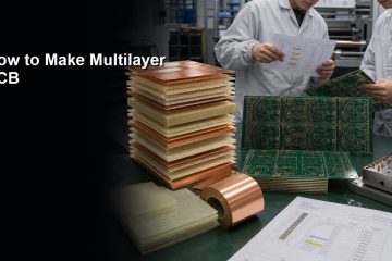
How to Make a Multilayer PCB: Stackup, Lamination and DFM Checks
See how multilayer PCBs are designed, imaged, laminated, drilled, plated, finished, and tested, plus the files and DFM checks needed before fabrication.



See how multilayer PCBs are designed, imaged, laminated, drilled, plated, finished, and tested, plus the files and DFM checks needed before fabrication.
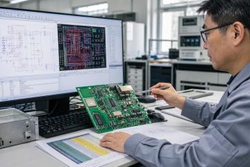
Evaluate a China PCB design service by defining inputs, stackup, DFM, review milestones, source-file ownership, and the final manufacturing handoff.
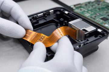
Learn how to make a flexible PCB by choosing the right stackup, protecting bend areas, preparing fabrication files, and checking the finished flex circuit.

Learn PCB design through three beginner projects, from schematic and footprints to layout, ERC/DRC, manufacturing files, DFM and first-board checks.
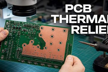
Learn when PCB thermal relief pads improve soldering, when solid connections are safer, and how to review spokes, current, vias and DFM rules.
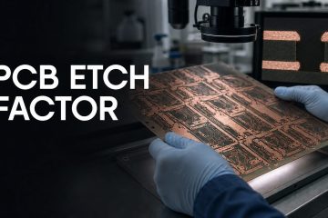
Learn how PCB etch factor changes finished trace width, impedance and fine-line DFM, with formulas, examples and fabrication checks.
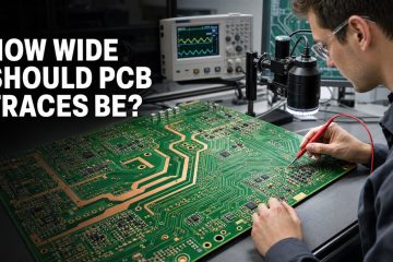
Learn how to choose PCB trace width from current, copper weight, temperature rise, voltage drop, impedance and fabrication limits.
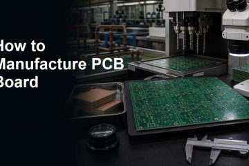
Learn how to manufacture PCB board from Gerber files through imaging, drilling, plating, solder mask, silkscreen, surface finish, inspection, and DFM checks.
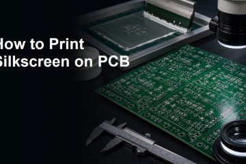
Learn how to print silkscreen on PCB with legend layers, pad clearance, useful markings, manufacturing limits, readability checks, and DFM review.
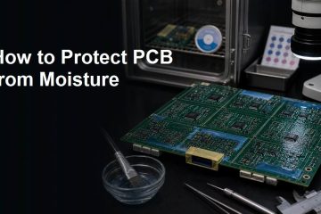
Learn how to protect PCB from moisture with design spacing, conformal coating, masking, cleaning, storage, inspection, and DFM review.
If you have any enquiry about quotation or cooperation, please feel free to email us at [email protected] or use the following enquiry form. Oursales representative will contact you within 24 hours. Thank you for your interest in our products.