




What Is PCB Thermal Relief?
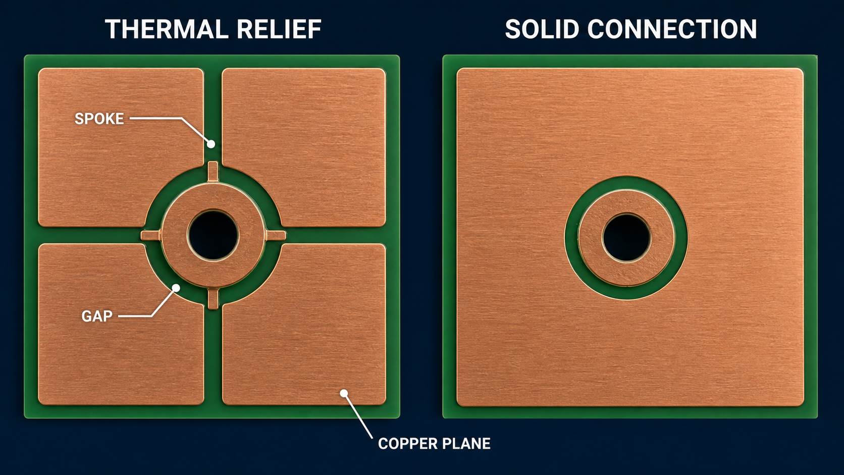
PCB thermal relief is a pad-to-plane connection made through a small number of copper spokes instead of a continuous ring of copper. The spokes limit how quickly a large copper area draws heat away during soldering while still providing an electrical connection.
The correct choice is not “use thermal relief everywhere.” A soldered through-hole pin may benefit from relief, while a high-current terminal, a non-soldered stitching via or an IC exposed thermal pad may need a solid connection. The component datasheet, current path, assembly method and fabricator’s design rules must agree.
Why Can a Solid Plane Make a Pad Difficult to Solder?
A solid copper plane acts as a heat sink. When a soldering iron, wave or reflow process heats the joint, the plane conducts part of that energy away. The pad can lag behind nearby pads, causing slow wetting, incomplete barrel fill, excessive dwell time or damage from an operator compensating with too much heat.
The risk is especially visible with through-hole ground pins, large copper pours and heavy copper. In reflow assembly, unequal thermal response between two ends of a small component can also contribute to wetting imbalance. Thermal relief reduces the local heat path; it does not correct poor stencil printing, pad geometry or an unsuitable reflow profile.
How Do Spokes, Gaps and Copper Weight Change the Result?
Spoke count and width control electrical, thermal and mechanical connection, while the air gap controls isolation from the surrounding pour. Wider or more numerous spokes lower resistance and move more heat. Narrower or fewer spokes make soldering easier but reduce current and heat-transfer margin.
| Design change | Soldering effect | Electrical/thermal tradeoff |
| More or wider spokes | Pad heats more like the plane | Lower resistance and stronger heat path |
| Fewer or narrower spokes | Pad reaches soldering temperature more easily | Less current and heat-transfer margin |
| Thicker copper | Greater heat sinking during assembly | Can support current but needs process-specific DFM |
| Larger relief gap | More thermal isolation | Consumes copper and clearance area |
Do not copy one spoke width from a web article. Minimum printable copper, etch compensation, finished copper, current, pad size and assembly process change the workable value.
PCB Thermal Relief vs Solid Connection: Which Should You Use?
Use thermal relief when solderability is the governing problem and the spokes can safely carry the required current. Use a solid connection when low resistance, heat spreading, RF return continuity or a component-specific exposed-pad layout is more important.
| Feature | Likely starting choice | Confirm before release |
| Soldered through-hole ground pin | Thermal relief | Barrel fill, current and wave/hand process |
| High-current connector pin | Solid or enlarged custom relief | Current, temperature rise and soldering method |
| Non-soldered stitching via | Usually solid | Return path, via function and plane continuity |
| IC exposed thermal pad | Follow datasheet; often solid copper and thermal vias | Stencil, via design and package guidance |
| RF or high-speed return connection | Often solid/low-inductance | Return-current path and field behavior |
| Hand-soldered low-current lead | Thermal relief | Iron access and joint acceptance |
How Should Through-Hole Pads and Plane Connections Be Reviewed?
For a plated through-hole pin, review every connected plane layer, not only the visible outer layer. Multiple solid plane connections can remove heat from the barrel and reduce solder rise. Conversely, a relief with inadequate copper may not meet current or mechanical needs.
- Identify which pins are actually soldered and which holes are only vias.
- Check relief on every connected internal and outer plane layer.
- Confirm annular ring and spoke attachment remain manufacturable after etching.
- Match the pattern to hand, selective or wave soldering.
- Define barrel-fill and joint criteria appropriate to the project.
Can Thermal Relief Spokes Carry the Required Current?
The spokes are parallel copper paths, so their finished width, thickness, length and temperature environment determine the available current margin. A plane capable of carrying high current does not help if the narrowest connection between the pad and plane is the relief pattern.
Calculate the connection using the finished copper geometry and acceptable temperature rise, then review abnormal current and fuse-like behavior. For heavy-copper or power designs, read the heavy copper PCB design guide and ask the fabricator to confirm the proposed pattern after CAM compensation.
Why Are IC Exposed Thermal Pads a Different Case?
An exposed thermal pad under a power IC is designed to conduct heat from the package into PCB copper. Adding ordinary spokes can defeat that heat-spreading function. Many component layouts instead specify a solid land, controlled paste apertures and an array of thermal vias, but the exact construction must follow the manufacturer’s datasheet.
Do not confuse “thermal pad” under a package with “thermal relief pad” around a solderable plane connection. They solve opposite thermal tasks: one moves operating heat away; the other limits heat loss during soldering.
When Can Thermal Relief Hurt Signal Integrity or Heat Flow?
Relief spokes can add inductance and interrupt a broad return path. The effect may matter for RF grounding, fast return currents, high-current switching loops or components that depend on uninterrupted copper for cooling.
Check the component reference layout and the actual current loop. A low-frequency connector ground and a microwave return via should not inherit the same default rule merely because both connect to GND.
Which Failures Suggest the Relief Pattern Is Wrong?
| Observed problem | Possible connection issue | What else to check |
| Slow wetting or low barrel fill | Too much solid copper or overly strong spokes | Flux, preheat, finish and soldering settings |
| Burned pad or long rework dwell | Plane removes heat too rapidly | Tool power, operator method and laminate damage |
| Tombstoning | Unequal copper/thermal connection at opposite pads | Paste volume, placement, pad symmetry and profile |
| Hot relief spokes in service | Insufficient current cross-section | Load, copper thickness and fault current |
| Power IC runs hot | Relief used where solid heat spreading was required | Datasheet land, paste voiding and thermal vias |
| RF/EMI problem | Return path narrowed by relief geometry | Stackup, loop area, stitching and reference plane |
What Should DFM Review Check Before Fabrication?
DFM review should verify that the intended electrical and assembly behavior survives polygon fill, CAM processing and etching. Supply Gerber or ODB++, drill data, stackup, finished copper, current requirements and assembly method.
- List soldered plane-connected pads and non-soldered vias separately.
- Flag high-current, RF and exposed-pad exceptions.
- Check spoke width and gap against finished copper and fabrication limits.
- Review inner-layer connections and antipad clearances.
- Check symmetry on small two-terminal components.
- Confirm the soldering process can heat any solid-connected exceptions.
The broader PCB DFM and DFA guide explains how this check interacts with pads, clearances, drilling and assembly access.
PCB Thermal Relief Release Checklist
- Component datasheet and reference layout reviewed.
- Current and temperature-rise requirement recorded.
- Soldering method identified.
- Thermal relief, solid and custom exceptions documented.
- Finished copper—not only starting foil—confirmed.
- Every connected plane layer reviewed.
- Non-soldered stitching/return vias checked separately.
- Exposed thermal pads checked for solid land, paste and via requirements.
- Fabricator confirms printable spokes and gaps after compensation.
- Assembly inspection criteria defined for critical joints.
FAQs About PCB Thermal Relief
Do all ground pads need thermal relief?
No. The correct connection depends on soldering, current, signal return and heat-spreading requirements.
Should stitching vias use thermal relief?
Usually a non-soldered stitching via uses a solid connection, but confirm its return-current and manufacturing role.
Can thermal relief cause voltage drop?
Yes, if the spoke cross-section is inadequate for the current. Review the finished geometry and allowable temperature rise.
Is four spokes always required?
No. Four is a common pattern, not a universal requirement. Pad size, current, copper and factory rules determine the design.
Does reflow assembly eliminate the need for relief?
Not automatically. Reflow can heat a board more uniformly than hand soldering, but thermal imbalance and package limits still matter.
Should a PowerPAD use thermal relief?
Follow the component datasheet. Exposed power/thermal pads commonly need efficient solid heat transfer rather than ordinary relief spokes.
Can a fabricator change thermal relief during CAM?
Only within agreed manufacturing rules. Critical current, RF or thermal exceptions should require engineering approval.
What files help a supplier review thermal relief?
Send copper data, drill files, stackup, finished copper, fabrication drawing, current notes and the assembly method.
Send Plane-Connection Rules for DFM Review
For a manufacturing review, send Gerber or ODB++, drill files, stackup, finished copper, current requirements, component datasheets and assembly method to [email protected]. Mark high-current terminals, RF returns and exposed thermal pads so PCBTRY can check whether the proposed relief and solid connections remain manufacturable before quotation.



0 Comments