




What Should a China Hard Gold PCB Quote Confirm?
A China hard gold PCB quote should confirm exactly where electrolytic hard gold is required, the nickel and gold requirements stated on the controlled drawing, the connector geometry, the inspection method, and which areas must remain solderable. A price without those details may describe a different plating scope, so it cannot be compared safely with another quote.
Hard gold is normally chosen for contact surfaces that face repeated mechanical wear, such as edge fingers, key contacts, test contacts, or mating pads. It should not be added to every exposed pad by default. Before asking for price, define the contact duty, mating direction, plated area, board-edge treatment, and acceptance evidence.

What Is Hard Gold Plating on a PCB?
Hard gold is an electrolytically deposited gold alloy applied over a nickel barrier on selected PCB contact areas. The alloying element increases surface hardness and wear resistance. That makes the finish useful where another connector repeatedly slides across the PCB surface.
The word “hard” describes the plated contact finish, not the stiffness of the circuit board. It is also different from jewellery plating and from the soft gold used for wire bonding. The fabrication drawing should use an unambiguous finish name and project-specific layer requirements instead of relying on the word “gold.”
When Should You Choose Hard Gold Instead of ENIG?
Choose hard gold when the plated surface is a mechanical contact; choose ENIG when the main requirement is a flat, solderable component-pad finish. They solve different problems and should not be treated as interchangeable gold colors.
| Decision point | Hard gold | ENIG |
| Main job | Wear-resistant mating contact | Flat solderable surface and storage protection |
| Typical location | Gold fingers, switch or test contacts | Component pads and general exposed copper |
| Deposition route | Electrolytic plating with electrical connection needed during processing | Electroless nickel followed by immersion gold |
| Design concern | Plating bars, selective area, edge geometry and wear duty | Pad finish compatibility and solder-joint process |
| RFQ question | Where, how measured, and what contact duty? | Which pads and which soldering/storage requirement? |
For more background on the solderable finish, see the ENIG PCB finish guide. A mixed-finish board may use hard gold on fingers and another finish on solder pads, but the drawing must separate the regions clearly.
Which PCB Areas Should Receive Selective Hard Gold?
Apply hard gold only to areas that need repeated contact or controlled low-contact resistance under mechanical wear. Common candidates include card-edge fingers, elastomer or spring contacts, keyboard contacts, test points designed for repeated probing, and connector lands.
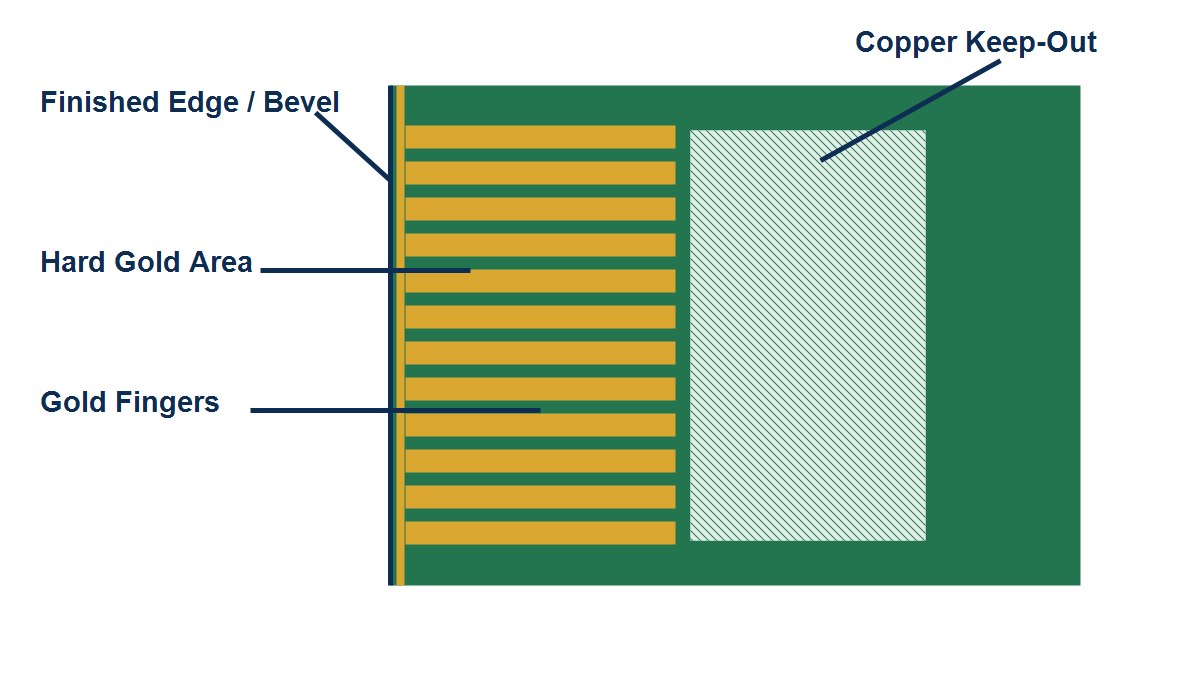
Mark the boundary as a manufacturing feature, not as a vague note. The fabricator needs to know whether the plated area stops before the solder mask, reaches the routed edge, includes a chamfered surface, or excludes nearby solderable pads. If different contact groups have different requirements, identify them with separate drawing callouts.
What Must the Fabrication Drawing Specify?
The fabrication drawing should control the finish in a way that survives file handoff and quotation. A Gerber image shows copper geometry, but it does not fully communicate plating composition, measurement location, or acceptance method.
| Drawing field | What to state | Why it matters |
| Finish name | Electrolytic hard gold over nickel; distinguish it from ENIG or soft gold | Prevents the wrong gold process |
| Selective area | Dimensions, layer side, finger/contact IDs and boundary | Controls plated scope and cost |
| Layer requirement | Project-approved nickel and gold requirement plus applicable specification | Creates a measurable acceptance condition |
| Edge treatment | Bevel angle/depth or square edge, tolerances and edge position | Controls connector insertion |
| Mask relationship | Mask opening and keep-out around the contact area | Prevents interference and exposed transitions |
| Inspection | Measurement method, sampling plan and report requirement | Makes supplier evidence comparable |
Include the note in the fabrication drawing and reference the same revision in the purchase order. The Gerber manufacturing-data guide explains why artwork alone cannot replace controlled fabrication notes.
How Should Gold Fingers Be Designed for Manufacturing?
Gold fingers need consistent width, spacing, alignment and distance from the finished board edge. The mating connector must engage the plated contact without scraping across solder mask, exposed copper, a via opening, or an uncontrolled transition.
- Keep vias, pads and copper features out of the bevel and routing risk zone unless the supplier approves the construction.
- Make the finished edge datum explicit and dimension finger length from that datum.
- Confirm whether shorter “first-mate/last-break” fingers are intentional.
- Identify non-plated gaps and solder-mask dams that must remain after routing.
- Provide the mating connector or its mechanical drawing when fit is critical.
Use the existing PCB gold finger design guide for a deeper geometry review before releasing files.
Why Do Bevels, Board Edges and Keep-Outs Matter?
The connector meets the finished board edge before it meets the electrical contact. A wrong bevel, excessive edge burr, shifted outline or copper too close to routing can damage the connector or change insertion force even when the plating itself passes inspection.
Define the bevel on a mechanical drawing with a datum, direction and tolerance. Ask whether routing occurs before or after the relevant plating steps and how the supplier protects the contact surface during depanelization. For array panels, confirm rail orientation and handling areas so clamps and tooling do not mark the fingers.
Which Plating and Solderability Risks Need Separation?
Hard gold is optimized for contact wear, not general solder-joint formation. Do not let a global finish note cause hard gold to be applied automatically to component pads. Separate contact regions from solderable regions in the drawing and quote.
Also confirm how the supplier makes the electrical connection required for electrolytic plating. Temporary plating bars or tie traces must be removed or left only where the design permits. Review the final CAD data after any engineering change, because an unapproved tie can create an electrical short or leave exposed copper at the cut point.
How Does Hard Gold Affect Cost and Lead Time?
Cost depends on plated area, layer requirements, selective masking, connector geometry, beveling, panel utilization, measurement and reporting—not simply on the board count. A small finger area with difficult selective processing can cost more per square centimetre than a larger, simpler surface finish.
Lead time can also change when the job needs a special plating route, test coupon, measurement report, tight mechanical edge, or first-article approval. Ask suppliers to separate one-time engineering/tooling items from recurring unit cost. Do not compare a quote that includes a thickness report with one that only says “hard gold.”
What Inspection Evidence Should the Supplier Provide?
Inspection evidence should connect the drawing requirement to a measured result. Request the method and sampling plan before production rather than asking for “100% quality” after the boards are finished.
- Visual inspection for pits, stains, scratches, exposed nickel, edge damage and inconsistent coverage.
- Layer-thickness measurement at defined locations using an agreed method.
- Finished outline, bevel and finger geometry measurements.
- Continuity and isolation test appropriate to the bare PCB.
- First-article photographs or report when connector fit is a project risk.
- Lot identification and report linkage when traceability is required.
Do not assume that a generic certificate proves the selected contact area meets your drawing. The evidence must identify the order, revision, lot and measured feature.
Which Defects Should a First Article Check Catch?
A first article should catch both plating defects and interface defects before volume production. The board can look gold and still fail mechanically or electrically.
| Observed issue | Possible cause to investigate | Buyer action |
| Uneven color or coverage | Plating distribution, surface preparation or masking variation | Compare mapped measurements and approved appearance criteria |
| Scratches on contact path | Handling, routing, packaging or fixture contact | Review protection and packaging method |
| Connector binds during insertion | Bevel, outline, thickness or finger alignment error | Measure against mechanical datum and test the actual connector |
| Exposed base metal near edge | Routing/plating sequence or insufficient edge allowance | Review cross-section/edge evidence and drawing boundary |
| Soldering problem on nearby pad | Wrong finish scope or contamination | Verify selective-finish map and process separation |
How Do You Compare China Hard Gold PCB Quotes?
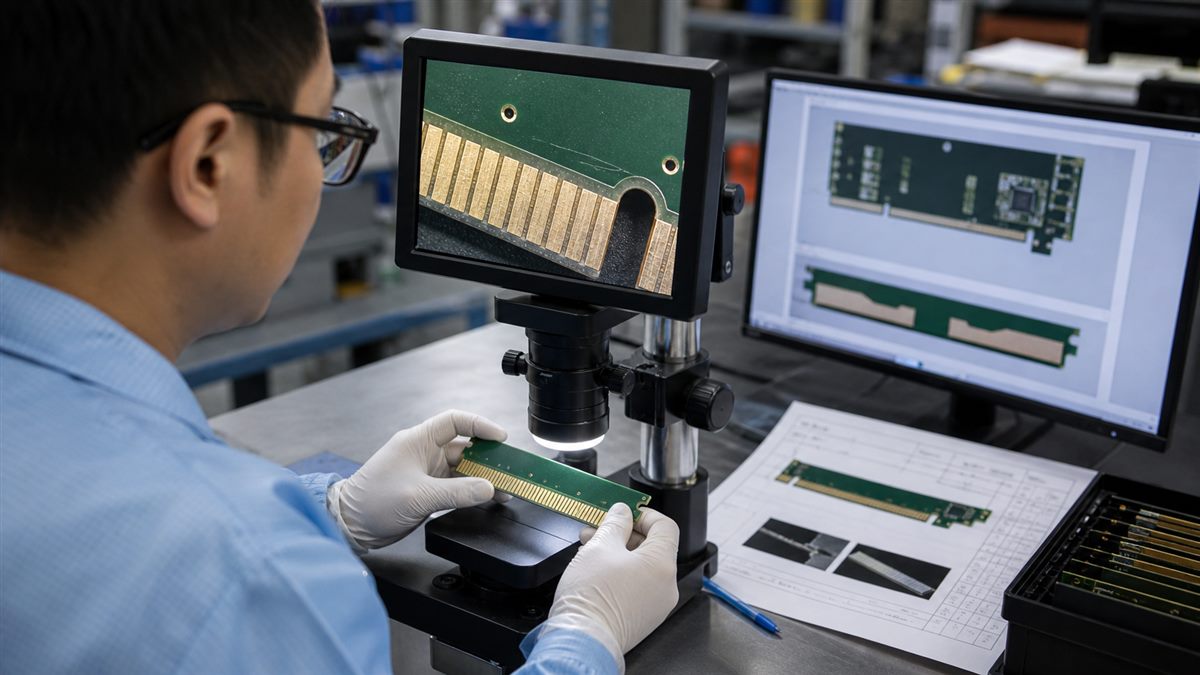
Normalize every quote to the same drawing revision and acceptance package. If one supplier quotes a selective contact area and another assumes the whole exposed surface, the totals answer different manufacturing questions.
- Confirm the same board quantity, panel delivery format and revision.
- Compare the same hard-gold area, nickel/gold requirement and applicable specification.
- Check whether beveling, selective masking, coupon and report costs are included.
- Confirm solderable finish on all non-contact pads.
- Compare electrical test, mechanical inspection and first-article evidence.
- Record approved substitutions or CAM changes before accepting price.
A structured PCB DFM review should resolve ambiguous plating boundaries before the purchase order is released.
China Hard Gold PCB RFQ Checklist
Send one controlled package so every supplier prices the same scope:
- Gerber or ODB++ data and NC drill files.
- Fabrication drawing with board revision and finished dimensions.
- Selective hard-gold area map and side/layer identification.
- Nickel and gold requirements plus the applicable project specification.
- Gold-finger dimensions, pitch, finished-edge datum and bevel requirement.
- Finished board thickness and connector-fit tolerance.
- Finish required on solderable pads outside the contact area.
- Electrical test, visual criteria and thickness-measurement request.
- First-article quantity and approval evidence.
- Production quantity, panel delivery preference and packaging protection.
- Any mating-connector drawing or fit sample.
- Required report, traceability and change-approval rules.
When Is PCBTRY a Practical Fit?
PCBTRY is a practical comparison option when your hard-gold PCB package includes controlled fabrication data, selective plating requirements and measurable acceptance needs. For a prototype or first build, the goal is to resolve plating bars, edge geometry, finish boundaries and inspection evidence before volume release. The China prototype PCB guide explains how to use that first build as a controlled production baseline.
Send the Gerber/ODB++ package, NC drill data, fabrication drawing, gold-finger detail, quantities and inspection requirements through the PCBTRY contact or quotation path. Ask for DFM feedback and a line-by-line confirmation of the hard-gold scope before approving production.
Frequently Asked Questions
Is hard gold the same as ENIG?
No. Hard gold is electrolytically plated and intended mainly for wear-resistant contact surfaces. ENIG is an electroless nickel and immersion-gold finish commonly used for flat solderable pads. A board may use both in different areas when the drawing defines the boundary.
Is hard gold used on every PCB pad?
Usually not. It is normally selective because component pads need a solder-compatible finish while fingers and contacts need wear resistance. Applying it everywhere can add cost and create an unsuitable soldering surface.
How thick should hard gold plating be?
There is no single thickness for every connector. Set the requirement from the mating system, wear duty, applicable specification and supplier capability, then state the approved nickel and gold requirements on the fabrication drawing. Do not copy an unrelated web number into the purchase order.
Does thicker gold always mean longer connector life?
Not by itself. Contact force, mating material, surface roughness, contamination, alignment, bevel quality and insertion cycle all affect wear. Validate the complete connector interface rather than treating thickness as the only reliability variable.
Why is nickel used under hard gold?
The nickel layer acts as a barrier and provides a suitable foundation for the gold contact surface. Its requirement and condition influence the finished interface, so it should be controlled with the gold layer rather than omitted from the drawing.
Can hard gold be soldered?
A hard-gold contact surface is not the default choice for component solder pads. If soldering near the contact area is required, define a separate solderable finish and obtain process approval for the exact geometry.
Do gold fingers always need a bevel?
No, but many card-edge connectors use a bevel to guide insertion. The need, angle and depth come from the connector and mechanical design. If no bevel is needed, state the finished edge requirement clearly.
What files are required for a hard-gold PCB quote?
Provide PCB artwork, drill data, a controlled fabrication drawing, the selective plating map, edge/bevel details, stackup or board construction, quantity, test requirements and inspection/report expectations.
How should hard-gold thickness be verified?
Agree on the measurement method, locations, sampling plan and report format before production. The report should link results to the order, revision and manufacturing lot.
What should be approved before mass production?
Approve the DFM changes, final fabrication drawing, plating boundaries, mechanical edge, first-article measurements, visual condition, electrical test and connector fit where it matters. Freeze the approved revision before repeating the build.



0 Comments