




A PCB gold plating process is not one universal sequence. ENIG builds electroless nickel and then deposits a thin immersion-gold cap without an external plating current. Electrolytic hard gold uses electrical current to deposit a wear-resistant gold alloy over nickel, normally on selected contacts such as card-edge fingers. If a drawing says only “gold plating,” the fabricator still does not know which route, function or acceptance evidence is required.
The practical task is to connect the finish to its job. Solderable component pads, sliding contacts, wire-bond surfaces and corrosion protection do not automatically need the same deposit. This guide explains the manufacturing branches, the controls that matter and the information a designer or buyer should put on a drawing or RFQ. It does not provide bath formulas or operating recipes; those belong to a qualified chemistry supplier and a controlled plating line.
First Decide What Gold Plating Means on This PCB
Begin with function, not color. ENIG is commonly selected as a flat, solderable finish: electroless nickel covers exposed copper, and immersion gold protects the nickel before assembly. Electrolytic hard gold is normally selected where a contact must withstand repeated mechanical engagement. Other nickel/gold families, including ENEPIG and soft electrolytic gold, have different layer systems and application boundaries.
PCBtry already has a general guide to PCB surface-finish selection and a separate explanation of electroless nickel immersion gold. Here, the focus is narrower: what happens during manufacture, what the designer must enable and how the result should be verified.
| Question | ENIG | Electrolytic hard gold |
|---|---|---|
| How is nickel deposited? | Autocatalytic electroless reaction on activated copper | Normally electrodeposited using an external current path |
| How is gold deposited? | Immersion displacement reaction on nickel | Electrodeposition from a controlled plating bath |
| Does the feature need electrical connection during gold deposition? | No external plating current | Yes; selected features need connection to the plating circuit |
| Primary design use | Flat solderable pads and multifunction finish applications | Wear contacts, especially card-edge fingers |
| What should the buyer define? | Applicable specification, finish category, measurement and acceptance plan | Contact function, nickel/gold system, selective area, thickness, alloy or hardness requirement, bevel and test evidence |
This comparison is a route-selection tool, not a complete specification. The relevant drawing and procurement requirements must govern the actual deposits.
ENIG vs Electrolytic Hard Gold: Process and Use Differences
The two routes may both appear gold at final inspection, but their deposition mechanisms create different manufacturing constraints. ENIG can coat isolated exposed copper features because it does not require a wired current path for each pad. Electrolytic hard gold cannot be treated as a purely chemical dip: current must reach the plated feature. That requirement affects artwork, panel rails, temporary connections and selective masking.
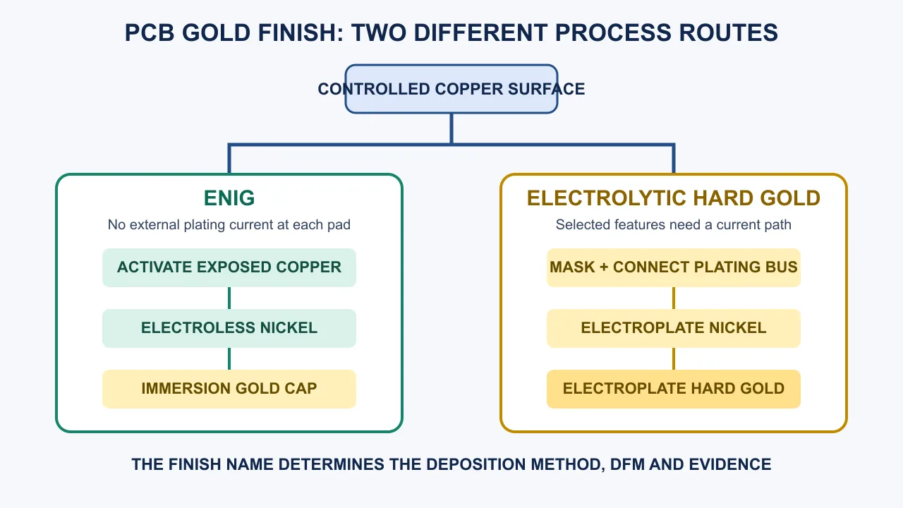
The gold also performs a different job. In ENIG, the thin immersion layer protects the nickel surface until interconnection. IPC-4552A describes ENIG as electroless nickel capped by immersion gold and makes process distribution, measurement accuracy and deposit uniformity central to conformance. For hard gold, the selected gold deposit is intended to tolerate contact wear; solderability should not be assumed merely because the surface is gold-colored.
A mixed-finish board may therefore use ENIG on component pads and electrolytic hard gold on connector fingers. That combination must be identified before CAM and panel planning. It is not a last-minute cosmetic option.
PCB Gold Plating Process Flow Before the Routes Split
Both routes depend on a controlled copper surface. Oils, oxides, solder-mask residue, fingerprints, roughness variation and poor rinsing can interfere with activation or deposit formation. A typical industrial flow therefore establishes these control objectives:
- Confirm the finish map. Identify which exposed areas receive ENIG, hard gold or another finish and which areas must remain protected.
- Inspect incoming surfaces. Check solder-mask definition, exposed copper condition, edge-finger geometry and evidence of contamination or damage.
- Clean and condition. Remove soils and prepare the copper using the qualified line sequence.
- Microetch and rinse as specified. Create the controlled surface condition required by the process, then prevent carryover into the next stage.
- Activate or connect the selected features. ENIG requires controlled activation for electroless nickel; electrolytic plating requires a verified electrical route and current distribution.
The exact chemicals, concentrations, dwell times and temperatures are line-specific. Copying a generic recipe from the internet would bypass the chemistry supplier’s process window, waste-treatment requirements and fabricator’s qualification evidence.
ENIG Process: Electroless Nickel Then Immersion Gold
After qualified pretreatment, the exposed copper is activated for electroless nickel deposition. The nickel-phosphorus layer grows without externally wiring each pad to a power source. It becomes the functional barrier and interconnection surface beneath the final gold.
The board is then rinsed and transferred to the immersion-gold stage. Immersion deposition is a displacement process: gold deposits as the underlying nickel participates in the reaction. The gold layer protects the nickel from oxidation during the intended handling and storage interval. Longer exposure is not simply “more is better”; the chemistry and deposit interface must remain within the controlled process.
Final rinsing and drying matter because residues and handling contamination can damage an otherwise acceptable deposit. Release evidence may include visual inspection, calibrated thickness measurement on agreed features, process-control records and application-specific solderability or other tests. The IPC-4552A scope and requirements should be read in its applicable contractual context rather than reduced to a single thickness number.
Electrolytic Hard Gold Process for Edge Contacts
Electrolytic hard gold begins with a manufacturable current path. The panel or coupon design connects the selected contact features to a plating rail or other controlled electrical bus. Areas that must not receive the deposit are protected with a selective mask or resist arrangement compatible with the fabricator’s process.
Nickel is electrodeposited first as an underplate and diffusion barrier. Hard gold is then electrodeposited on the specified contact area using a qualified alloy and process. Current density and current distribution influence deposition, so feature geometry, location on the panel, electrical continuity and masking are process inputs—not administrative details.
After plating, temporary mask material is removed and the panel is cleaned. Temporary plating connections may be removed during profiling. Edge contacts can also require a controlled bevel, setback and geometry so the connector mates without exposing a vulnerable edge or damaging the contact. PCBtry’s existing guide to hard-gold PCB and gold-finger RFQ checks provides additional sourcing context.
Why Plating Buses, Masking and Panel Design Matter
An isolated finger cannot receive electrolytic gold unless the manufacturing design provides electrical continuity during plating. Fabricators may add temporary traces, thieving, panel rails or other CAM features, but the acceptable method should be resolved before production. Otherwise, later removal can leave copper exposure, alter the finished edge or conflict with routing and bevel requirements.
Selective masking must also define the transition between hard gold and adjacent finishes. Ask where the mask boundary can fall, what positional tolerance applies and whether the mixed-finish sequence has been reviewed. When component pads and connector fingers share copper geometry, treating the finishes as a color choice can create a process conflict.
A useful DFM review therefore answers three questions: Can current reach every hard-gold feature? Can the temporary connection be removed without violating the finished drawing? Can masking and later processing maintain the required finish boundary? If any answer is uncertain, stop release and obtain the fabricator’s panel proposal.
Quality Controls and Evidence at Each Process Stage
| Stage | Main risk | Evidence to review | Release decision |
|---|---|---|---|
| Drawing and CAM | Wrong finish or unplateable isolated feature | Finish map, plating connection and selective-mask review | Release only when route and boundaries are explicit |
| Pretreatment | Soil, oxide, residue or uneven copper condition | Line controls, representative inspection and rinse control | Do not plate a visibly or measurably unsuitable surface |
| Nickel deposition | Skips, roughness, poor adhesion or thickness variation | Process records, calibrated measurement and representative coupon evidence | Hold if distribution or interface evidence is outside the agreed plan |
| Gold deposition | Incomplete coverage, nonuniformity or interface attack | Bath/process controls, appearance screening and thickness evidence | Appearance alone cannot release the lot |
| Rinse and dry | Carryover, stains or handling contamination | Rinse controls, cleanliness and final visual inspection | Investigate residues rather than polishing away evidence |
| Finished board | Finish meets color expectation but not function | XRF where applicable, solderability, contact, adhesion, microscopy or other drawing-required tests | Accept against the contracted criteria and sampling plan |
X-ray fluorescence can provide non-destructive deposit information, but a reading is meaningful only with suitable calibration, feature geometry, measurement location and method. IPC-4552A explicitly ties conformance to process control, measurement accuracy and uniform deposit characteristics. A buyer should request the evidence needed for the application, not an impressive-looking certificate with no connection to the drawing.
Common Gold-Finish Defects: What to Check Before Blaming the Bath
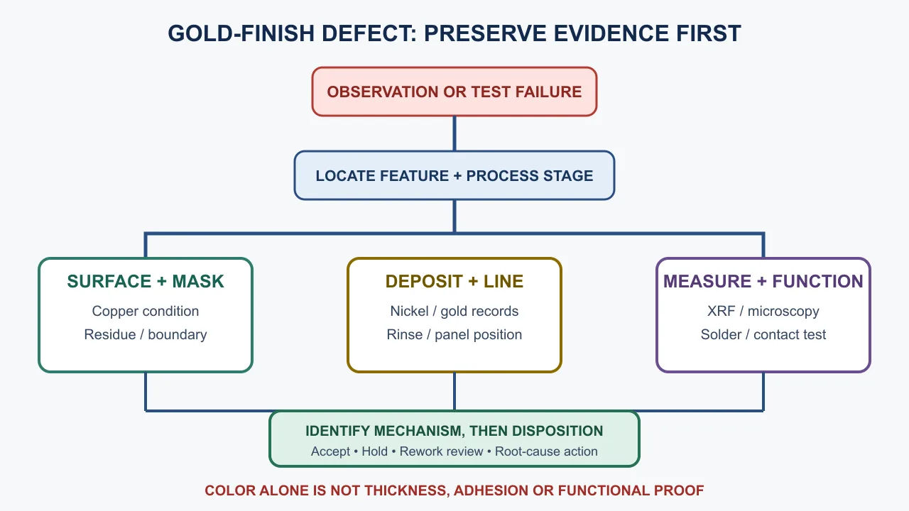
| Observation | Possible mechanisms | Discriminating check | Response |
|---|---|---|---|
| Skip or exposed area | Mask residue, poor cleaning, activation failure, interrupted current path or local geometry | Compare affected locations with finish map, mask boundary and electrical continuity | Hold the lot and isolate the failing stage |
| Rough or nodular surface | Incoming copper roughness, contamination, particles or uncontrolled deposition | Inspect preplate surface and compare process/coupon evidence | Do not assume the gold bath is the only cause |
| Stain or discoloration | Rinse carryover, drying, handling contamination or deposit variation | Review rinse records and characterize the surface before cleaning it | Preserve evidence; avoid abrasive rework without disposition |
| Thickness variation | Feature geometry, measurement setup, bath distribution or current distribution | Repeat calibrated measurements at agreed locations and compare panel position | Evaluate against the sampling and specification plan |
| Solderability concern on ENIG | Deposit/interface condition, contamination, storage or assembly variables | Correlate finish evidence with representative solderability and assembly history | Use cross-functional root-cause analysis |
| Early connector wear | Wrong finish family, insufficient functional deposit, rough mating system or geometry issue | Verify drawing, deposit evidence, bevel and connector conditions | Do not replace a wear system with generic ENIG by assumption |
The table deliberately lists several mechanisms per symptom. A gold-colored surface can hide a nickel, copper, masking, rinsing, measurement or design problem. Root-cause work should preserve samples and records from adjacent stages.
Published Process-Control Case: ENIG Thickness and Measurement
Problem: An ENIG specification needs deposit limits that fabricators and customers can reproduce, but thickness results depend on process distribution and measurement capability—not only a nominal target.
Treatment and action: An IPC-hosted final-finish specification review describes round-robin work involving suppliers, PCB manufacturers, EMS providers and OEMs. The work compared deposit results and informed ENIG specification requirements. IPC-4552A subsequently emphasizes controlled process distributions, accurate and reproducible measurement, uniform deposit characteristics and defined measurement-feature context.
Result: The published record supports specification-based acceptance and controlled measurement rather than a color check or an isolated reading. It does not prove that every ENIG line, feature size or application produces the same result, and it does not set the hard-gold requirement for a particular connector.
Reader lesson: Put the applicable finish specification, measurement conditions and acceptance plan into the supplier agreement. A number without finish identity, feature context and measurement control is not a complete requirement.
How to Specify PCB Gold Plating on a Drawing or RFQ
Write the finish name in full and identify where it applies. If the board uses mixed finishes, provide an unambiguous map and resolve the process order with the fabricator. State the functional objective—soldering, wear contact, wire bonding or another controlled use—because it determines what evidence matters.
Reference the applicable specification and revision where one is contractually required. Define nickel and gold requirements in the form used by that specification or agreed drawing, including measurement locations and sampling. For hard-gold fingers, also address selective area, contact length, allowable mask transition, bevel, edge condition and any hardness, wear or contact-resistance evidence required by the product.
Finally, define how deviations are handled. Substituting ENIG for hard gold, changing alloy, moving the finish boundary or altering the measurement feature should require review rather than silent acceptance.
PCB Gold Plating RFQ and Quality Checklist
Saveable general work aid: copy or print this checklist before releasing a gold-finish PCB. It is not an IPC specification, process qualification, test report or guarantee; apply the governing drawing and standards.
- Name the finish completely: ENIG, electrolytic hard gold, ENEPIG, soft electrolytic gold or another defined system.
- State the functional purpose for each finished area.
- Mark every selective-finish boundary on the drawing or controlled fabrication note.
- Reference the applicable specification and revision.
- Define nickel and gold requirements without mixing values from different finish families.
- Agree the measurement method, feature size/location and sampling plan.
- Confirm electrical access, plating rails and removable connections for electrolytic features.
- Review masking tolerance and the sequence when more than one finish is used.
- Define edge-finger geometry, setback and bevel where applicable.
- Identify required solderability, adhesion, contact, wear or microscopy evidence.
- Set packaging, handling and storage requirements appropriate to the finish.
- Require approval before any finish, alloy, thickness, boundary or test substitution.
Frequently Asked Questions
Is PCB gold plating the same as ENIG?
No. ENIG uses electroless nickel followed by immersion gold. “Gold plating” can also mean electrolytic hard gold, soft gold, ENEPIG or another defined nickel/gold system.
What is the main process difference between ENIG and hard gold?
ENIG does not require an external plating current at each pad. Electrolytic hard gold uses current, so the selected features need a manufacturable electrical path during deposition.
Why is nickel placed under gold on a PCB?
Nickel provides the functional barrier and interconnection surface between copper and gold. Its deposit condition is therefore as important as the visible gold cap.
Can ENIG be used on gold fingers?
ENIG can appear on contacts, but it should not automatically replace electrolytic hard gold where repeated mating wear is a design requirement. Select the finish from the connector specification and use conditions.
Does a thicker gold layer always make a better PCB?
No. The correct deposit depends on finish family, function, specification and process capability. Uncontrolled extra deposition can change cost and interface behavior without proving better performance.
How is PCB gold thickness checked?
XRF is commonly used for non-destructive deposit measurement, but calibration, feature geometry, measurement location and the applicable method determine whether the result supports acceptance.
What causes uneven hard-gold plating?
Possible contributors include current distribution, electrical connections, geometry, masking, surface condition and process control. Compare panel location and records before changing one bath parameter.
What causes black-pad concerns in ENIG?
The term relates to an abnormal nickel/gold interface condition and should not be diagnosed from color alone. Preserve samples and examine deposit, process, storage and assembly evidence.
Can ENIG and hard gold be used on the same PCB?
Yes, a mixed-finish design is possible when the fabricator can control sequence, electrical access, masking and boundaries. It must be planned during DFM, not added as an ambiguous note.
What should a PCB gold-plating RFQ include?
Include finish identity, functional area, specification, layer requirements, selective boundaries, measurement and sampling plan, connector geometry and any application-specific test evidence.
Turn the Finish Name into a Manufacturable Requirement
The best gold-plating decision is not “gold or no gold.” It is a controlled match between deposition route, feature function, panel design and acceptance evidence. Send PCBtry the finish map, connector drawing, stackup, applicable specification and inspection requirements for a manufacturability review. Specialized finish capability and final process limits must be confirmed for the actual order.



0 Comments