




A 5V label does not define one PCB-layout problem. The rail may enter through USB, arrive from another board, come from a linear regulator, or be generated by a switching converter. Each case creates different current paths, heat sources, noise risks and validation needs. Good 5V power supply PCB layout therefore starts by identifying what the rail does—not by copying a generic capacitor placement.
What Does 5V Power Supply PCB Layout Mean for Your Board?
Before moving footprints, record the source, allowed input range, output tolerance, steady and transient load, regulator topology, switching modes, board stackup, connector context and test criteria. The word “5V” states a nominal voltage; it does not state current, allowable voltage drop, ripple, thermal rise or EMC performance.
A 5V rail feeding a quiet sensor is different from one powering LEDs, motors, relays or a processor with fast load steps. A USB-derived rail also has an interface boundary: the connector, cable, protection, inrush behavior and permitted source current all matter. If the board generates 5V, the regulator data sheet and its reference layout become controlling documents.
| 5V rail role | Primary layout question | What must be verified |
|---|---|---|
| 5V input from connector | How does current enter, return and reach loads? | Source limits, protection, cable drop, bulk/local decoupling and shared return paths |
| USB-derived 5V | Does the power path respect the applicable interface and product architecture? | Connector, protection, inrush/backfeed behavior and actual negotiated or permitted current |
| LDO-generated 5V | Are input/output capacitors and heat paths correct for that LDO? | Data-sheet capacitance/ESR conditions, dropout, dissipation and stability requirements |
| Buck-generated 5V | Are pulsed-current loops and switching copper controlled? | Local input loop, switch node, inductor/output path, feedback reference and thermal design |
| Shared 5V distribution rail | Can one load disturb another through common impedance? | Branch current, local energy storage, return continuity, connector/via limits and load-step response |
Start With the 5V Power Path and Regulator Topology
Mark the complete path on the schematic: source, protection, input capacitors, regulator, switching devices or pass element, inductor where applicable, output capacitors, connector or load, feedback network and ground references. Then mark the corresponding copper and layer transitions on the placement drawing.
This exercise prevents a common mistake: optimizing individual traces while missing the loop that carries the changing current. An LDO has no switch node, but capacitor connection and heat dissipation still matter. A buck converter has switching-state-dependent current paths. A boost or buck-boost converter has a different hot-loop location. An isolated supply introduces transformer, primary/secondary return and safety boundaries. Do not transfer a buck-specific drawing unchanged to another topology.
Use the selected IC data sheet—not a generic blog diagram—to resolve pin-specific details such as AGND/PGND treatment, exposed-pad connection, feedback pickup and recommended component placement. Analog Devices’ AN-136 and Texas Instruments’ buck-converter EMI layout guidance explain why current-loop geometry and parasitic inductance matter, but the chosen regulator documentation remains the design-specific authority.
For a Buck Output, Map the Local Switching Loop First
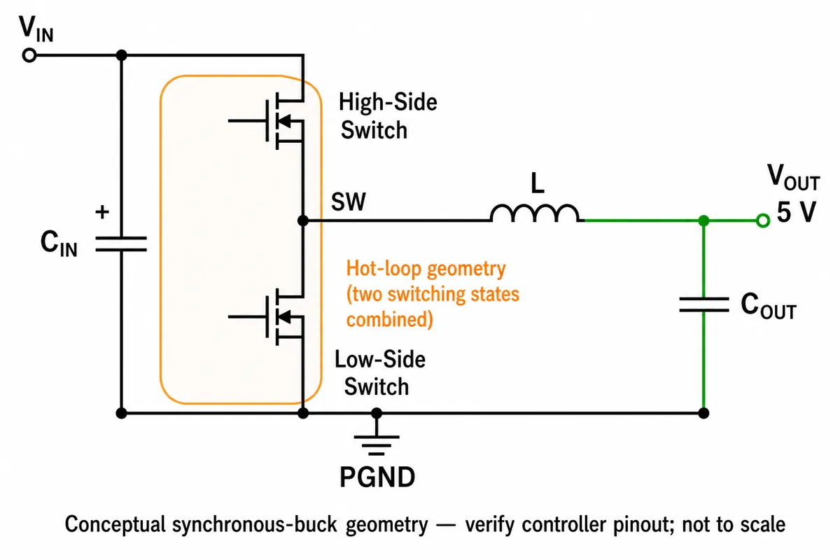
In a synchronous buck, the high-side and low-side switches conduct during different switching states. The illustration combines those states only to show the compact physical region around the local input capacitor and switching devices; it does not mean both switches should conduct simultaneously.
The local input ceramic capacitor must connect to the relevant VIN and power-return pins with low parasitic inductance. “Close” should be judged electrically: pad geometry, trace length and width, vias, layer changes and the return path all count. A nearby capacitor connected through a long detour may be less effective than it appears in the top-view placement.
Keep the required switch-node connection intact, but avoid enlarging high-dv/dt copper without a justified reason. The switch node must connect the switching device to the inductor; it is not a general heat-spreading plane. Excess area can increase capacitive coupling to adjacent conductors and structures. The optimum balance depends on device loss, thermal needs, package and manufacturer guidance.
Place Local Decoupling by Electrical Connection, Not Visual Distance
Local bypass capacitors provide a short path for fast current changes. Bulk capacitance addresses slower energy demand and cable/source impedance. Those functions overlap, but they are not interchangeable. A large capacitor at a connector does not automatically replace the small local capacitor required at a regulator or load IC.
For every important capacitor, inspect both terminals. Trace the current from the source or device pin into the capacitor and back through its reference. Check whether vias or plane voids enlarge the loop. Confirm effective capacitance at the applied DC bias, temperature and tolerance—not only the nominal value printed in the bill of materials. Also confirm the IC’s permitted capacitor type and ESR range because some regulators depend on those characteristics for control-loop behavior.
Keep Switching Copper and Quiet Measurements Separate
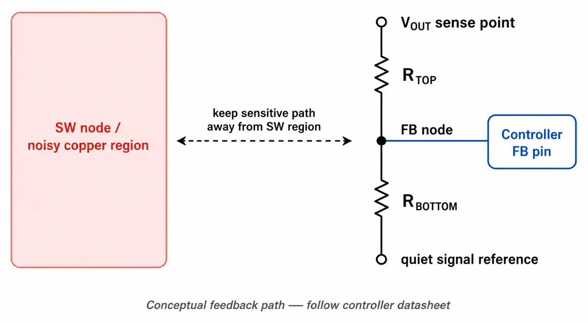
A feedback divider is a measurement circuit. Its upper resistor senses the regulated output; the divider node connects to the controller FB pin; and the lower resistor returns to the controller-defined quiet reference. The correct pickup and reference locations vary by architecture. Do not connect VOUT directly to an adjustable FB input unless the data sheet explicitly defines that arrangement.
Route feedback, compensation and current-sense conductors away from the switch node, gate-drive paths and other high-field regions. Avoid placing unrelated copper under or beside a switch node without understanding the capacitive coupling. If a sensitive trace changes layers, review the nearby return path and reference-plane continuity rather than considering only the signal trace.
These practices support lower coupling risk, but they do not prove EMC compliance. For broader board-level controls, see our guide on how to reduce EMI in PCB design.
Choose the Ground and Return Strategy From the Controller Guidance
Ground is a current-return network, not decorative copper. Identify which currents return through the local input capacitor, output capacitor, protection parts, connector and exposed pad. Review where power ground and quiet signal reference meet and whether common impedance lets switching current disturb the sensed voltage.
A universal “split ground” rule is unsafe. A split can force return current around a void, while an uncontrolled solid plane can still share noisy and sensitive paths. Follow the controller’s PGND, AGND and exposed-pad recommendations, then verify the actual current geometry on every relevant layer. If the manufacturer shows a single-point connection or a particular pad/via arrangement, understand which current it controls before adapting it.
Review USB, Connectors and Shared 5V Loads as a Boundary
When 5V enters through USB or another connector, the connector is part of the power system. Check source capability, cable resistance, protection devices, inrush, hot-plug behavior, reverse current/backfeed risk and connector contact rating. Do not assume that every USB-shaped connector provides the same current or that a laboratory supply reproduces the field cable and source.
For a shared rail, separate branch currents conceptually. A motor, relay or LED load may create steps that appear at a sensor or digital IC through shared trace and return impedance. Place local energy storage where it serves the intended load, keep disruptive branches from sharing sensitive return segments where practical, and define how the board behaves during brownout or current limiting.
Size Copper, Vias and Thermal Paths From the Real Load
Voltage alone does not size copper. Use continuous and peak current, duty cycle, waveform, copper thickness, layer, path length, permitted temperature rise, via construction and the PCB fabricator’s capability. A short 5V logic branch and a multi-ampere 5V distribution path require different treatment even though the nominal voltage is identical.
Review connectors, fuses, protection devices, vias and neck-downs as part of the same current path. A wide plane can still be limited by a narrow pad exit or a small via array. For the necessary inputs and limitations, use the PCB trace-width guide.
Thermal performance also depends on loss, package, copper spreading, thermal vias, neighboring heat sources, airflow and enclosure. Do not claim a junction temperature from copper area alone. Where an exposed pad is used, follow its land-pattern and via guidance and coordinate solder-paste and assembly requirements. Our thermal-via design guide explains the fabrication variables that must be reviewed with the supplier.
Where These 5V Layout Decisions Apply
USB-powered sensor or controller: begin at the connector and protection boundary. Check the permitted source behavior, cable drop, inrush/backfeed controls and local load transients. If a downstream regulator creates another rail, treat that converter as a separate power stage rather than assuming the incoming 5V capacitor serves every load.
Buck-generated 5V for digital loads: map the local input switching geometry, switch node, inductor/output path and feedback reference. Then inspect how a processor, radio or other fast load connects to the 5V output and return. The regulator reference layout guides the power stage; the load data sheets guide local decoupling.
LDO-generated 5V for a quieter branch: there is no buck switch node, but input/output capacitor connection, effective capacitance, ESR conditions, dropout and heat still require review. Estimate dissipation from the actual input-output difference and current, then validate temperature under the intended board and enclosure conditions.
Shared 5V rail for mixed loads: identify branches with large or abrupt current demand and keep them from disturbing sensitive loads through common trace or return impedance. Measure at the source and critical loads during representative events instead of assuming that a nominal 5V reading at one test point describes the whole board.
A Published Example: Input Decoupling Can Change the Diagnosis
Texas Instruments documents a converter evaluation-module test in its 2018 Power Supply Design Seminar paper Common Mistakes in DC/DC Converters and How to Fix Them. During a large load step, long bench-supply leads or insufficient input bypassing produced input-voltage variations that also appeared as output oscillation. That response could be misdiagnosed as poor loop stability.
The treatment in the published example was to add sufficient bulk input decoupling at the evaluation module. TI reports that the input disturbance and corresponding output oscillation were eliminated in the shown load-step response. In a second documented condition near minimum input voltage, the input dip crossed the converter’s undervoltage-lockout threshold, causing shutdown and restart.
This is not a universal capacitor value or a guaranteed result for a 5V board. It demonstrates a reusable diagnostic lesson: the source, cable, local input network, load step and probe setup are part of the observed system. Before changing compensation, verify whether the input rail is being disturbed by the test fixture or power-path impedance.
Use a Review Sequence That Produces Evidence
- Classify the rail. State whether 5V is an input, output, USB-derived rail or internal distribution rail.
- Freeze operating assumptions. Record input range, load profile, transient cases, ambient, airflow, enclosure and acceptance criteria.
- Mark current paths. Map the topology-specific pulsed loop, continuous output path and return paths on both schematic and layout.
- Check component placement. Compare the actual pin-to-pad geometry with the selected regulator’s reference layout.
- Inspect sensitive routing. Verify feedback pickup, quiet reference, compensation and sensing paths against switching copper.
- Review manufacturability. Check stackup, copper, vias, thermal land pattern, mask, paste, test access and supplier constraints.
- Plan measurements. Define load, probe method, bandwidth, test point, temperature method and pass/fail limits before bring-up.
Download the 5V Power Supply PCB Layout Review Sheet (PDF). It is an original, source-based planning worksheet—not a test report, certification, manufacturer data sheet or universal layout recipe. Its final page lists the public technical sources used to build it.
Validate Before Calling a 5V Rail Quiet or Stable
Before fabrication, review the schematic, regulator documentation, stackup, placement, routing and DFM output together. During bring-up, record input source, cable, load condition, operating mode, probe connection, bandwidth, test point, board revision and acceptance limit. Use a short ground spring or suitable differential method where required by the measurement; a long oscilloscope ground lead can add misleading ringing.
Check startup, shutdown, no-load, steady load and relevant load steps across the intended input and temperature range. Observe the 5V rail at the regulator and at critical loads. Record component and board temperature under defined conditions. EMC, stability, safety and lifetime claims require appropriate analysis and testing; a clean-looking layout is not evidence by itself.
FAQ: 5V Power Supply PCB Layout
Is every 5V supply a buck-converter layout?
No. First identify whether 5V is an input, regulated output, USB-derived rail, LDO rail or switching rail. Each topology has different critical paths.
Where should a buck input capacitor go?
Follow the selected controller’s VIN and power-ground reference layout so the electrical pulsed-current loop is compact. Inspect both capacitor terminals and any vias.
Can trace width be chosen from 5V alone?
No. Current waveform, copper thickness, layer, path length, temperature-rise target, via construction and fabrication capability determine the required geometry.
Should feedback connect directly from VOUT to FB?
Not as a general rule. Adjustable regulators normally use a controller-specific divider and reference arrangement. Follow the exact data sheet and reference design.
Does a ground pour automatically solve noise?
No. The actual return paths, plane continuity, shared impedance and connection of power and quiet references must be reviewed.
How should I handle a USB-derived 5V rail?
Apply the requirements appropriate to the actual USB architecture and source, including connector, protection, inrush, backfeed and permitted-current behavior.
What should stay away from a switch node?
Keep feedback, compensation, current sensing and other noise-sensitive conductors away according to the controller guidance. Do not enlarge switch-node copper without justification.
How many decoupling capacitors does a 5V rail need?
There is no universal count. Use the regulator and load-device data sheets, then verify effective capacitance, bias, temperature, tolerance, placement and source impedance.
Why can a 5V rail dip during a load step?
Possible causes include source or cable impedance, insufficient effective capacitance, layout parasitics, current limiting, control response or load-path voltage drop. Measure both input and output before assigning a cause.
Can I use the same layout for an LDO and a buck regulator?
No. An LDO has no switching hot loop or switch node, while a buck regulator does. Both still require data-sheet-compliant capacitor and thermal placement.
How should I measure 5V ripple?
Document the load, test point, probe type, ground connection and bandwidth limit. Use a low-inductance probing method so the setup does not create apparent ringing.
When should a PCB manufacturer review the layout?
Before release, when the stackup, copper weights, via construction, thermal features, mask/paste details and actual operating assumptions are available.
Get the 5V Power Layout Reviewed Before Fabrication
If your 5V rail must support a defined load, connector, regulator or thermal target, send PCBtry the schematic, component data sheets, stackup request and operating envelope. We can review manufacturability and layout-critical constraints before the design is committed to fabrication. Electrical performance still depends on the complete design and must be confirmed with appropriate engineering validation.



0 Comments