




The PCB cutting process creates the finished board outline and, when boards are manufactured in arrays, separates individual boards from the production panel. Manufacturers use CNC routing, V-scoring, saw cutting, punching, or laser processing according to the outline, laminate, thickness, component position, volume, and edge requirement. The choice matters because an acceptable drawing can still produce chipped edges, dimensional errors, exposed fibers, cracked solder joints, or damaged components if the panel and separation method are not designed together.
PCBtry reviews the profile layer, panel drawing, material, stackup, component-edge clearance, tolerance, and inspection notes before selecting a cutting route. Send Gerber or ODB++ data, the fabrication drawing, panel requirements, assembly data when populated panels are involved, and the acceptance standard to request a DFM review and quotation.
What Does PCB Cutting Include?
PCB cutting includes two related jobs: profiling a bare board or manufacturing panel to its designed geometry, and depaneling individual boards after fabrication or assembly. CNC routing may perform both jobs, while a V-groove is normally prepared during bare-board production and separated later with controlled equipment. Mixing these stages in a drawing can leave the supplier unsure whether a line represents a finished edge, a routed slot, a score, or an assembly break line.
The release package should distinguish the finished board outline from panel rails, routed channels, breakaway tabs, mouse-bite holes, V-score lines, internal cutouts, and plated or unplated slots. It should also state whether the manufacturer may optimize panelization or must follow a customer-controlled array.
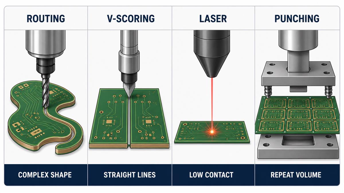
Which PCB Cutting Method Fits the Design?
The best method is the one that meets geometry, stress, cleanliness, edge, and volume requirements without creating a new reliability risk. No method is automatically best for every PCB.
| Method | Best fit | Main control | Important limitation |
|---|---|---|---|
| CNC routing | Curved outlines, complex profiles, mixed shapes, and routed tabs | Tool path, fixture support, bit condition, dust extraction, and final dimensions | Tool diameter limits internal corners; worn tools can roughen or delaminate edges |
| V-scoring | Straight, continuous lines across regular rectangular arrays | Score alignment, remaining web, board support, and controlled separation | Only straight lines; bending strain can reach components, vias, or solder joints near the score |
| Laser cutting | Thin, flexible, intricate, or mechanically sensitive parts after process validation | Material-specific energy, focal control, residue, heat effect, and edge inspection | Material response and edge condition must be qualified; a consumer laser is not an acceptable substitute |
| Saw cutting | Straight-line singulation on compatible products | Blade condition, alignment, cooling/extraction, and support | Geometry is restricted and mechanical loading must be evaluated |
| Punching or die cutting | Stable geometry at repeat volume where dedicated tooling is justified | Tool alignment, wear, clearance, and crack/burr inspection | Tooling locks the geometry and applies mechanical force |
| Controlled manual separation | Low-risk prototypes with correctly designed breakaway features | Fixture, direction, support, and inspection | Operator variation and bending make it unsuitable for many dense or reliability-critical assemblies |
How Does the PCB Cutting Process Work?
The factory process connects drawing interpretation, panel design, machine setup, cutting, cleaning, and inspection so that the final edge is traceable to the approved data.
Step 1: Review the profile and acceptance notes. CAM engineering checks outline continuity, internal cutouts, slots, radii, tolerance, datum, edge plating, bevels, and separation instructions. An open contour or duplicate line can send a tool down the wrong path.
Step 2: Select the cutting and separation route. The engineer compares geometry, material, board thickness, copper near the edge, assembly state, component clearance, volume, and acceptable stress. A mixed process may use routing for curved edges and V-scoring for straight array lines.
Step 3: Design the production panel and supports. Rails, tabs, tooling holes, fiducials, coupons, and fixture-contact areas are added or reviewed. The panel must remain stable through imaging, plating, solder mask, assembly, and separation.
Step 4: Program and verify the equipment. The approved profile is converted into a controlled route, score, laser, saw, or punch program. Tool compensation, cut sequence, entry/exit position, and support are checked against the released revision.
Step 5: Run a first-piece cut. The first panel is cut or scored under controlled settings. Operators check dimensions, edge condition, tab or score behavior, and any sign of excessive vibration, heat effect, cracking, or laminate damage before releasing the lot.
Step 6: Separate the board with controlled support. For populated panels, the fixture and separation sequence keep the PCB flat and avoid transferring force into nearby ceramic capacitors, connectors, BGAs, or solder joints.
Step 7: Remove debris and finish permitted tab remnants. Routing dust, loose fibers, and allowed tab nubs are managed without sanding into copper, solder mask, edge plating, or a controlled finished dimension.
Step 8: Inspect and release. The factory verifies profile dimensions, slots, corner features, edge finish, delamination, chips, exposed conductors, plated-edge continuity where applicable, and damage to populated assemblies. Nonconforming boards remain segregated until disposition.
How Should Panelization Support Cutting?
Panelization should hold the board securely during fabrication and assembly while leaving a predictable, low-risk separation path. Rails provide handling and tooling space; tabs retain routed boards; V-scores create straight fracture lines; fiducials and tooling holes keep the array aligned.
Tab positions should not concentrate force beside fragile components, narrow necks, edge connectors, antennas, or copper features. Mouse-bite perforations trade easier break-off for a visible remnant that may require controlled finishing. If an enclosure needs a flush edge, define the allowed tab-remnant condition instead of assuming hand finishing will meet the fit.
Review the complete panel rather than only the individual PCB. PCBtry’s guide to PCB panelization with rails, V-scores, and tabs explains the upstream decisions that make cutting stable.
How Do Material and Stackup Change Cutting?
Material and stackup change tool wear, heat response, dust, fracture behavior, stiffness, and edge quality. Standard FR-4 can expose glass fibers or delaminate if a router tool is worn. Thin flex circuits need support and often benefit from a validated non-contact or dedicated die process. Metal-core boards require a route suitable for the metal layer and insulation interface. Ceramic substrates are brittle and need a qualified singulation strategy rather than an FR-4 assumption.
Thick copper, copper near the profile, edge plating, castellations, embedded features, and asymmetric stackups also change the risk. The fabrication drawing should identify the material system and every special edge feature; the supplier should confirm the proposed tool and inspection route before production.
What Causes Edge and Depaneling Defects?
Most defects come from a mismatch among the drawing, panel support, material, tool condition, or separation force. The failure record should show both the physical defect and the process control that failed.
| Defect | Likely cause | Prevention/control | Buyer checkpoint |
|---|---|---|---|
| Rough edge or exposed fibers | Worn router, unstable feed, poor support, or uncontrolled break-off | Tool-life control, stable fixture, qualified cut direction, and edge inspection | Approved edge sample and visual criteria |
| Delamination or chipping | Excess mechanical load, unsuitable tool, material damage, or poor entry/exit control | Material-specific route and first-piece validation | Magnified edge inspection and nonconformance record |
| Wrong outline dimension | Tool compensation, datum, revision, or program error | Program verification and calibrated measurement | First-article dimensional report |
| Cracked component or solder joint | Board bending during V-score or tab separation | Low-strain layout, support fixture, controlled equipment, and strain validation when required | Component-edge review and post-separation inspection/test |
| Damaged copper or edge plating | Profile data conflict, finishing beyond limit, or unprotected plated feature | Explicit drawing and controlled route | Cross-section, continuity, or visual evidence as specified |
| Laser residue or heat effect | Unqualified laser/material combination | Parameter study, extraction, cleaning, and edge acceptance | First-piece edge images and cleanliness criteria |
How Are Dimensions and Edge Quality Verified?
Verification should measure the features that affect fit and reliability, using the drawing datum and stated acceptance method. A coordinate measuring system, optical measurement equipment, gauges, or other calibrated tools may be used according to geometry and tolerance. The report should identify the drawing revision, measured locations, equipment, and result.
Visual inspection checks fibers, burrs, chips, delamination, burns, cracks, tab remnants, solder-mask damage, and exposed copper. Internal corners and routed slots deserve special attention because tool diameter and compensation affect the result. Edge plating or castellations need their own continuity, coverage, and damage criteria. A generic “outline passed” note is weaker than a first-article report tied to controlled characteristics.
How Does Cutting Affect Assembled Components?
Post-assembly depaneling can flex the board and transfer strain into solder joints and brittle components. The risk rises when components sit close to a V-score or breakaway tab, when a long board is unsupported, or when an operator twists the panel by hand. Damage may be latent even when the board powers on immediately.
During DFM, review component orientation and distance relative to the separation line, fixture-contact areas, connector overhang, heat sinks, and heavy parts. For risk-sensitive products, the team may use strain measurement, controlled router depaneling, or product-specific validation. The correct acceptance evidence depends on the assembly and reliability requirement; it should not be invented after a field failure.
What Files and Notes Should the Buyer Send?
A complete release package removes ambiguity before the supplier writes the cutting program.
- Gerber or ODB++ data with one unambiguous profile layer.
- Fabrication drawing with finished dimensions, datums, tolerances, slots, cutouts, bevels, edge plating, castellations, and special edge notes.
- Customer-controlled panel drawing, or written permission for supplier panelization.
- Assembly drawing and placement data when separation occurs after component mounting.
- Material, stackup, overall thickness, copper construction, and surface-finish requirements.
- Allowed tab-remnant, edge appearance, cleanliness, dimensional-report, sampling, and test requirements.
- Quantity, prototype/production stage, packaging need, and enclosure fit constraint.
How Should You Compare PCB Cutting Capability?
Compare how suppliers control your actual outline and assembly risk, not how many machine names appear on a website. Ask which method they propose and why, what design limits require confirmation, how tools and programs are controlled, how populated panels are supported, and what first-article evidence will be delivered.
Also ask how a process change is approved, how nonconforming edges are segregated, and whether dimensional and visual results remain traceable to the lot. For laser, metal-core, ceramic, thick, flex, plated-edge, or component-dense boards, request an engineering review before treating a quotation as a production commitment.
Frequently Asked Questions
Is PCB cutting the same as PCB depaneling?
Not exactly. Cutting may create the bare-board profile, slots, and panel features; depaneling specifically separates individual boards from an array, often after assembly. One project can use the same router for both stages, but the fixtures, stress risks, and acceptance checks differ.
When should V-scoring be used?
V-scoring fits straight, continuous separation lines on regular arrays when the layout and components tolerate the separation method. Confirm the score construction, remaining web, component clearance, support, and final edge requirement with the manufacturer.
When is routing preferred?
Routing is commonly preferred for curved or irregular outlines, internal cutouts, and tab-routed arrays. It offers flexible geometry, but tool radius, wear, dust, vibration, tabs, and fixture support must be controlled.
Does laser cutting eliminate all PCB damage?
No. Laser cutting avoids mechanical contact, but material response, residue, carbonization or heat effect, focus, and extraction still require validation. The supplier should approve the exact laminate and show first-piece edge evidence.
Can populated PCB panels be separated by hand?
Only when the product and panel are designed for a controlled low-risk break. Hand twisting can bend the board and damage components or joints near the separation line. Dense, fragile, or reliability-critical assemblies usually need controlled support and equipment.
What causes mouse-bite tabs to leave rough edges?
The perforated tab intentionally leaves a remnant after separation. Hole pattern, tab position, separation direction, laminate behavior, and finishing method determine the result. Define the allowed remnant when enclosure fit or touch safety matters.
How is a PCB outline tolerance checked?
The factory measures controlled profile locations from the drawing datum with calibrated equipment suited to the geometry. Put the tolerance and reporting requirement on the fabrication drawing; do not rely on a general website capability value.
What should be included in a PCB cutting quotation?
Include profile data, fabrication and panel drawings, material/stackup, board thickness, quantity, assembly state, component placement when populated, edge features, tolerances, inspection requirements, and any enclosure-fit or cleanliness constraint.
Request a PCB Cutting and Panel DFM Review
Send PCBtry your Gerber or ODB++ package, fabrication drawing, panel plan, stackup, material, quantities, component placement data when relevant, and edge acceptance requirements. The engineering review can identify whether routing, V-scoring, laser, or a mixed process fits the geometry and what inspection evidence should accompany the quotation.



1 Comment
PCB Milling Process: Routing Tools, Tolerances and Edge Quality Checks - thindry pcb manufacturer · 09/01/2026 at 15:14
[…] support fine features in suitable materials but introduces material/process constraints. PCBTRY’s PCB cutting process comparison helps select the […]