




The PCB edge plating process deposits conductive metal on a selected board sidewall and connects it to designed copper features on the top, bottom, or internal structure. It is used for chassis grounding, EMI shielding, mechanical/electrical contact, module edges, and other designs that need a metallized profile. Unlike a normal routed edge, the profile must be prepared, metallized, protected through later processing, finished, and inspected as an electrical feature.
PCBtry reviews the edge-plating drawing, wrap geometry, layer connections, profile tolerance, material, board thickness, surface finish, panel support, and inspection requirement before release. Send Gerber or ODB++ data, fabrication drawing, stackup, quantities, finish, and acceptance notes for a DFM review and quotation.
What Is PCB Edge Plating?
PCB edge plating—also called edge metallization, side plating, or wrap-around plating—covers a defined board edge with copper and usually the specified final finish. The copper normally wraps onto designed outer-layer lands so the sidewall metal has a robust connection and a measurable geometry.
It is not automatically the same as castellated holes, card-edge fingers, plated slots, or copper exposed accidentally by routing. Each feature needs a distinct drawing callout and manufacturing route.
Why Do Designs Use Plated Board Edges?
Designers use plated edges to connect a board perimeter to ground or a metal enclosure, reduce seam impedance in shielding structures, create a contact surface, or strengthen a specified interface. The plated edge only works when its electrical connection, mechanical fit, finish, and continuity match the application.
How Should Edge Plating Be Specified?
Show every plated segment on a dimensioned mechanical/fabrication drawing and identify the connected nets or copper lands. State the finished outline tolerance, wrap requirement, surface finish, plated and non-plated transitions, keep-outs, bevels, castellations, and inspection standard.
Do not rely on a note that says only “plate all edges.” The supplier needs to know where plating starts/stops and whether corners, slots, internal cutouts, tabs, or breakaway rails are included.
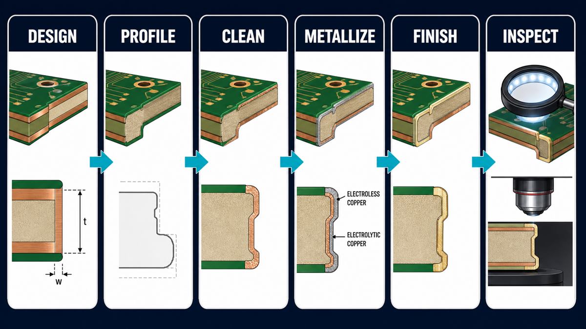
How Does the PCB Edge Plating Process Work?
The process keeps the intended sidewall accessible to metallization while preserving panel support and final geometry.
Step 1: DFM and data review. CAM checks the profile, wrap copper, net connection, corners, tolerance, panelization, and finish.
Step 2: Build and register the multilayer panel. Inner layers, lamination, drilling, and standard preparation establish the structure that the edge will connect.
Step 3: Prepare the selected profile. The factory routes or otherwise opens the edge at the controlled stage while retaining sufficient tabs/rails for later processing.
Step 4: Clean and activate the sidewall. Debris, smear, and contamination are removed so metallization can adhere.
Step 5: Deposit and electroplate copper. Conductive seed copper and subsequent plating connect the sidewall to the designed wrap lands.
Step 6: Image and etch the outer layers. The required edge connection and adjacent circuitry are preserved through the outer-layer process.
Step 7: Apply mask and final finish. Mask clearances and the specified finish protect/contact the intended areas without coating prohibited surfaces.
Step 8: Final profile and inspection. Remaining tabs are removed under control; dimensions, wrap, coverage, adhesion, finish, continuity, and edge damage are verified.
How Do Profile and Panelization Affect Plating?
The selected edge must be exposed early enough to receive copper, yet the board needs rails or tabs to remain stable through wet processing and handling. Tab positions cannot interrupt critical plated segments or leave unacceptable remnants.
Final routing can cut through plated copper if the sequence or tool path is wrong. Review panelization together with the finished outline; PCBtry’s PCB panelization guide explains rails, tabs, and V-score decisions.
Why Are Copper Wrap and Adhesion Important?
Wrap copper anchors the sidewall metallization to designed surface copper and creates a controlled current/ground path. Without adequate design and processing, edge copper may peel, crack, thin at the corner, or separate during final routing and assembly.
The required wrap geometry and copper acceptance must come from the project standard and supplier capability. Avoid copying a universal dimension from another fabricator’s website.
Which Surface Finishes Can Be Used?
The final finish depends on contact function, solderability, corrosion environment, wear, assembly, and cost. ENIG or other finishes may be considered, but not every finish/process route treats vertical edges identically.
Specify the finish and functional purpose, then ask the manufacturer to confirm edge coverage, masking, rack/contact marks, thickness evidence when required, and compatibility with later soldering or enclosure contact.
What Edge-Plating Defects Matter?
| Defect | Cause | Risk | Evidence/control |
|---|---|---|---|
| Peeling/lifted copper | Poor preparation, weak wrap, mechanical damage | Open ground/contact, loose metal | DFM, adhesion/visual inspection |
| Thin/voided coverage | Poor activation or current distribution | High resistance/corrosion | Cross-section or thickness evidence |
| Cracked corner | Geometry, stress or final routing | Intermittent connection | Magnified corner inspection |
| Wrong plated segment | Drawing/CAM ambiguity | Short, fit or shielding failure | First-article drawing comparison |
| Finish skip/stain | Process or contamination issue | Contact/solderability risk | Coverage and finish inspection |
| Dimensional error | Route compensation/sequence | Enclosure mismatch | Calibrated dimensional report |
How Is Edge Plating Inspected?
Inspection should verify the drawing, segment location, finished dimensions, visual coverage, wrap, corner condition, adhesion, continuity, and final finish. Cross-sections or thickness measurements may be required for controlled edges; electrical continuity alone cannot reveal weak adhesion or a marginal corner.
Define the standard revision, sample plan, measurement locations, cosmetic limits, continuity method, and report before quotation.
What Affects Cost and Lead Time?
Cost and schedule rise when edge plating requires special panelization, early routing, additional handling, selective masking, unusual finish, tight dimensions, many short segments, internal cutouts, cross-sections, or dedicated inspection. Material and board thickness can also change preparation and support.
A complete drawing lets the supplier quote the real route. Late edge-plating notes often force CAM revision, panel redesign, or a production restart.
What Should Buyers Send for an Edge-Plating Quote?
- Gerber/ODB++, NC drill/rout and dimensioned fabrication drawing.
- Clearly marked plated segments, net connection and wrap lands.
- Stackup, material, copper, thickness and quantities.
- Finished profile tolerance, corners, cutouts, tabs and allowed remnants.
- Surface finish, mask keep-outs, contact/solder/shield function.
- Inspection standard, continuity, thickness/cross-section and report needs.
Related processes include PCB cutting and depaneling and PCB copper plating.
Frequently Asked Questions
Is edge plating the same as castellated holes?
No. Castellations are plated holes cut through at the edge; continuous edge plating metallizes a defined sidewall. A design may contain both, but each needs its own data and acceptance.
Can every PCB edge be plated?
Not automatically. Geometry, material, panel support, wrap lands, corners, finish, tabs and supplier process determine feasibility.
Does edge plating require wrap copper?
A controlled wrap is normally important for robust connection and adhesion. The exact requirement must match the applicable standard and fabricator capability.
Can V-scored edges be edge plated?
A V-score is not automatically a suitable plated sidewall. The factory must review how the edge is opened, plated, supported and finally separated.
Can internal cutouts be plated?
They may be possible with a qualified route, but access, solution flow, geometry, panel support and inspection differ from an outer edge.
Which finish is best?
Choose from contact, solder, corrosion, wear, assembly and cost requirements; confirm actual edge coverage with the supplier.
How is plated-edge continuity tested?
The edge can be included in a defined electrical network test or measured by a specified method. Add visual/structural checks because continuity alone does not prove adhesion.
What files are needed?
Provide fabrication data, profile/rout data, stackup, dimensioned edge-plating drawing, finish, quantities and acceptance requirements.
Request an Edge-Plating DFM Review
Send PCBtry the complete fabrication package and explain whether the plated edge is for shielding, grounding, contact, soldering, or mechanical integration. Engineering can review wrap, panel support, profile sequence, finish, and inspection before quotation.



0 Comments