




The PCB milling process uses CNC routing tools to create the final board outline, slots, cutouts, notches and tab features after the panel has been fabricated. In prototype shops, “PCB milling” can also mean removing surface copper to isolate traces; production PCB profiling is a different operation with different data, tools and acceptance controls.
PCBTRY reviews the rout layer, fabrication drawing, panel layout, finished dimensions, plated/non-plated slots and edge requirements before programming. Send Gerber or ODB++, drill/rout files, drawing, stackup, quantity and controlled-dimension notes for DFM and quotation.
What Is the PCB Milling Process?
Production milling removes laminate with a rotating cutter following compensated CNC paths. The cutter has a finite diameter, runout and wear rate, so internal corners cannot be perfectly sharp and narrow slots must match an available qualified tool. The operation must preserve copper clearance, plated features, edge finish and dimensional datums.
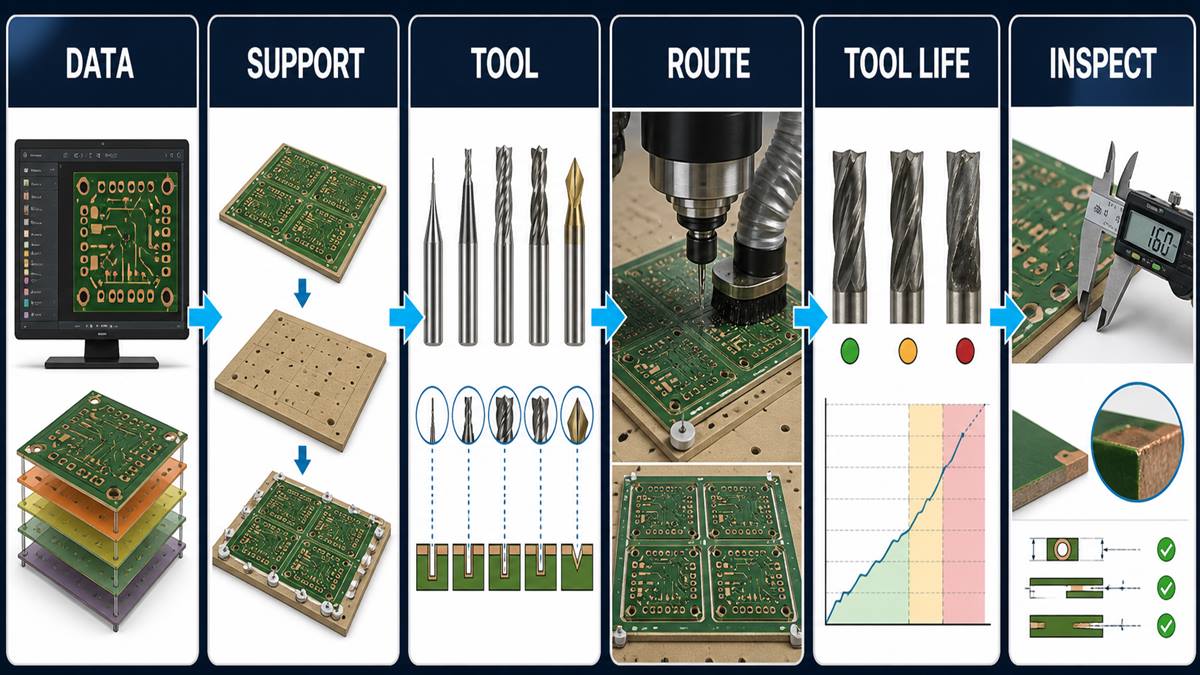
How Does the PCB Milling Process Work?
1. Rout-data and drawing review. CAM compares the profile layer, rout file and fabrication drawing. Conflicting outlines, undefined slots or ambiguous centerline/finished-edge data cause the wrong tool path.
2. Panel and support planning. The supplier places rails, tabs, tooling holes and support so boards remain stable during cutting. Too little support lets the part vibrate or move; poor tab placement can damage sensitive edge features.
3. Tool and path selection. Cutter diameter, flute geometry and coating are selected for laminate, copper, slot width and edge requirement. CAM applies tool-radius compensation and determines entry, direction and sequence.
4. Machine setup and datum verification. Spindle condition, collet, runout, panel height and registration are checked. A small tool with excessive runout can cut oversize, chatter or break even when the NC path is correct.
5. Routing/milling. Qualified spindle speed, feed, plunge and depth are used for the material/tool combination. Feeding too fast overloads the tool; feeding too slowly can rub, heat the resin and accelerate wear.
6. Tool-life control. The factory tracks distance, panel count or edge-quality indicators and replaces the cutter before unacceptable wear. A dull tool causes burrs, fiber breakout, heat marks and dimension drift.
7. Tab removal and edge cleaning. Remaining tabs or mouse bites are removed using the released process without gouging the final outline. Dust and loose fibers are cleaned.
8. Dimensional and visual inspection. Profile, slots, notch location, corner radii and edge defects are checked against the drawing. Critical dimensions require a defined datum, method and sampling plan.
Which PCB Features Are Commonly Milled?
| Feature | Key DFM question | Common risk |
|---|---|---|
| Outer profile | Which edge/datum controls size? | Oversize, undersize or edge burr |
| Internal cutout | Is the corner radius acceptable? | Impossible sharp corners |
| NPTH slot | Can the selected cutter make the width? | Width/position drift |
| Plated slot | Is it routed before plating and clearly identified? | Missing or damaged plating |
| Breakaway tab | Where can residual material remain? | Component/edge damage |
| Edge connector/bevel zone | Are profile and finish sequences compatible? | Scratched contacts or chipped bevel |
Why Can’t Milling Create Perfectly Sharp Internal Corners?
A rotating cylindrical cutter leaves an internal radius approximately related to its tool radius and runout. A CAD drawing with a zero-radius internal corner is not automatically machinable. Add a permitted radius, dog-bone relief or a different manufacturing method based on the mating part.
How Do Feeds, Spindle Speed and Tool Wear Affect Edges?
Cutting quality depends on chip load, laminate abrasiveness, copper content, tool geometry, runout and dust extraction. Universal RPM/feed values are unsafe because machines and materials differ. The supplier should use a qualified recipe and monitor edge quality rather than copy a hobby setting.
| Symptom | Possible cause | Control/evidence |
|---|---|---|
| Fiberglass burrs | Dull tool, poor support or wrong feed | Tool-life record and magnified edge check |
| Dark/heat-marked edge | Rubbing, heat or poor extraction | Recipe review and visual limit |
| Chipped laminate | Vibration, entry/exit path or damaged tool | Fixture/path and edge inspection |
| Dimension drift | Tool wear, runout or wrong compensation | First-piece and periodic measurement |
| Copper exposed at edge | Insufficient copper-to-profile clearance | CAM clearance check |
How Does Milling Differ from V-Scoring and Laser Cutting?
Routing supports irregular outlines, slots and cutouts but consumes panel space and cycle time. V-scoring is efficient for straight shared edges but leaves a controlled residual web. Laser cutting can support fine features in suitable materials but introduces material/process constraints. PCBTRY’s PCB cutting process comparison helps select the method.
How Should Copper and Components Be Kept Away from the Rout?
Clearance must cover tool-path tolerance, profile tolerance, plating/finish sequence and mechanical damage risk. Do not place copper based only on the nominal CAD line. Identify intentionally exposed edge copper or edge plating separately; otherwise CAM may treat it as a clearance error.
For plated edges, coordinate the route and metallization sequence described in PCBTRY’s edge plating process.
What Should Buyers Inspect?
- Finished profile against drawing datums.
- Slot width, length and location.
- Internal corner radius and mating clearance.
- Burrs, loose fibers, chips, scorch marks and exposed copper.
- Tab remnants and depaneling damage.
- Plated-slot or edge-plating continuity where specified.
- First-article and periodic dimensional records for critical features.
Panel and tab decisions should be reviewed with the PCB panelization guide.
PCB Milling FAQ
Is PCB milling the same as isolation routing?
No. Isolation milling removes copper for rapid prototypes; production milling usually profiles finished laminate and creates slots/cutouts.
What files define the board outline?
Send a dedicated rout/profile layer plus a fabrication drawing with datums and controlled dimensions. Resolve conflicts before tooling.
Why are inside corners rounded?
The cutter has a finite radius. Specify an allowed corner radius or relief based on the mating geometry.
What causes PCB edge burrs?
Tool wear, runout, poor support, incorrect feed/speed or unsuitable tooling can contribute. Inspect and correct the process, not only sand the symptom.
Can very narrow slots be milled?
Only if a qualified cutter and process support the width, depth and material. Ask the supplier before locking the drawing.
How are critical dimensions controlled?
Define the datum, finished dimension/tolerance and inspection method. First-piece plus periodic checks can monitor drift.
Does routing happen before or after plating?
It depends on the feature. Plated slots/edges require a process sequence different from ordinary final profiling.
What is needed for quotation?
Send fabrication data, drill/rout, drawing, stackup, copper weights, edge requirements, quantity and inspection/report needs.
Request a Milling and Profile DFM Review
Send PCBTRY your complete fabrication package and controlled mechanical drawing. Engineering can review tool access, corner radii, slots, copper clearance, panel support and inspection requirements before production.



0 Comments