




The PCB prototyping process is a controlled cycle that turns a design package into a small number of boards, then uses fabrication, assembly and test evidence to decide what must change before the next revision or pilot build. Its purpose is not merely to obtain boards quickly; it is to answer defined electrical, mechanical, thermal, firmware and manufacturing questions with minimum ambiguity.
A useful prototype begins with a written validation objective and production-relevant files. For DFM and quotation, send Gerber or ODB++, NC drill data, stackup and impedance requirements, fabrication drawing, BOM, CPL/centroid, assembly drawings, approved substitutions, programming files and a test plan.
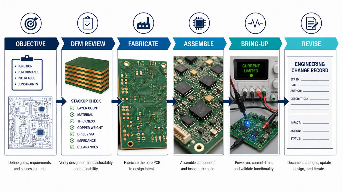
What Is the PCB Prototyping Process?
PCB prototyping covers more than bare-board fabrication. It starts when the engineering team decides what the build must prove, continues through design release, DFM, fabrication and optional assembly, and ends with measured verification and a documented release or respin decision.
A proof-of-concept may accept temporary wiring and non-final mechanics. An engineering prototype should be close enough to the intended stackup, materials, components and thermal environment for the results to be meaningful. A pilot build goes further by checking whether the process, inspection and test coverage can scale.
How Does the PCB Prototyping Process Work?
All stages belong to one learning loop. Skipping a stage may make the board arrive sooner but usually makes the result harder to interpret.
1. Define the build objective and exit criteria. State whether the prototype must prove power architecture, firmware boot, RF behavior, mechanical fit, thermal margin, sensor accuracy, assembly feasibility or another outcome. A board that “turns on” is not a pass unless the target measurements were defined beforehand.
2. Freeze and review the release package. Give the schematic, PCB data, BOM, CPL, drawings, stackup and test files one version identifier. Verify footprints, pin 1, package variants, connector orientation, mounting holes, enclosure datum and output plots. Mixed file revisions are a common cause of builds that are manufactured correctly but represent the wrong design.
3. Perform DFM, DFA and DFT review. DFM checks fabrication geometry, stackup, drills, copper, mask and outline. DFA checks polarity, spacing, stencil access, panel handling and rework risk. DFT checks test points, programming access and how each critical rail or interface will be observed. A generic CAD DRC cannot replace process-specific review.
4. Confirm materials, stackup and substitutions. Approve the laminate family, copper weights, dielectric structure, surface finish and impedance plan. For assembly, decide which component substitutions are allowed. A prototype built with materially different parts or stackup may work but fail to answer the production question.
5. Fabricate and electrically test the bare boards. Imaging, lamination, drilling, plating, etching, mask, finish and routing follow the approved traveler. The supplier should preserve the stackup and important inspection data. Bare-board electrical test checks the fabricated netlist before component value and solder variables are introduced.
6. Assemble the controlled first article. Verify BOM revision, component identity, moisture/handling needs, stencil data, polarity and first-piece placement. Inspect the first assembled board before releasing the remaining quantity when the design or package risk justifies it. Rework should be recorded rather than hidden because it changes how test results are interpreted.
7. Bring up the board incrementally. Inspect before power, check resistance to ground, use a current-limited source and verify primary rails before installing every optional module or enabling full loads. Then confirm clocks, reset, programming and communications. This sequence protects the board and creates a fault boundary when something is wrong.
8. Execute the verification matrix. Record expected value, test method, condition, result and pass/fail criterion for every objective. Include mechanical fit, thermal behavior, functional load, interfaces and firmware where relevant. A screenshot without test conditions is weak evidence.
9. Classify findings and decide the next build. Separate design defects, fabrication/assembly defects, test setup problems, firmware issues and approved prototype-only deviations. Create redlines and an engineering change record. Do not order a new revision merely because the first defect was found; finish safe testing so the next spin incorporates all known corrections.
What Files Prevent Prototype Delays?
| Package | What it controls | Frequent gap |
|---|---|---|
| Gerber/ODB++ and NC drill | Copper, mask, legend, profile and holes | Old drill file or ambiguous plated holes |
| Stackup/impedance table | Materials, layer order and controlled structures | Target given without reference layer or tolerance |
| Fabrication drawing | Thickness, finish, tolerances and special features | Drawing conflicts with data |
| BOM and approved alternates | Component identity and sourcing | Incomplete MPN or unapproved substitution |
| CPL and assembly drawings | XY, rotation, side and polarity | CAD origin/rotation mismatch |
| Programming/test package | Bring-up and measurable acceptance | No fixture access or expected readings |
How Should DFM Change a Prototype?
DFM should not silently redesign the circuit. It should identify a constraint, explain the manufacturing consequence and present an approved disposition: accept, revise, use a controlled deviation or change the process. Typical review areas include annular rings, drill-to-copper spacing, mask dams, copper balance, board edge clearance, panel rails, fine-pitch apertures and test access.
Record every approved deviation. Otherwise the next engineer may copy a prototype-only concession into production without understanding why it existed. Stage-specific reviews also matter; for example, our PCB lamination process guide shows how stackup decisions become factory controls and inspection evidence.
What Should a First-Article Build Verify?
| Question | Evidence | Decision it supports |
|---|---|---|
| Was the intended design built? | Version match, BOM/CPL and inspection record | Continue testing or stop the lot |
| Is the bare board electrically correct? | Netlist test and critical dimension checks | Separate fabrication from assembly faults |
| Can the board power safely? | Resistance, current-limit and rail sequence log | Proceed to clocks/firmware |
| Does it fit the product? | Connector, enclosure and mounting measurements | Mechanical revision |
| Can it be assembled repeatedly? | AOI/X-ray/visual and rework record | Footprint, stencil or process change |
| Does it meet the prototype objective? | Verification matrix under stated conditions | Pass, conditional pass or respin |
How Do You Bring Up a Prototype Safely?
- Confirm the board and BOM revision.
- Inspect polarity, bridges, debris and rework.
- Measure resistance on input and power rails with power off.
- Use current limiting and verify the primary power tree.
- Confirm reset, clocks and programming access.
- Enable interfaces and loads one block at a time.
- Record expected and measured values at named test points.
Plan these checks before fabrication so probes, fixtures and headers are accessible. Our circuit-card assembly testing guide explains the coverage gaps between inspection, ICT and functional testing.
What Prototype Failures Actually Teach You?
A failed test is useful only when its cause is classified. A footprint error requires library control; a solder bridge may require stencil or spacing changes; a collapsed rail can be design, placement or component related; an enclosure collision needs a datum correction. Avoid labeling every issue “manufacturing” before comparing the released files, inspection record and measured board.
Preserve one representative unit before extensive rework. Photographs, X-ray, resistance values and failure symptoms can disappear after components are removed. If rework is needed to continue validation, mark the change on the schematic and board drawing so results from the modified unit are not treated as original-design evidence.
When Is a Prototype Ready for Pilot Production?
- All prototype objectives have a recorded result and disposition.
- Critical design changes are incorporated into one controlled revision.
- Stackup, materials and substitutions are production-relevant.
- Known rework is eliminated or converted into an approved process.
- Assembly inspection and test coverage have defined acceptance criteria.
- Yield-sensitive features have supplier agreement and evidence.
- Fabrication, assembly, firmware and test files share the same release identifier.
Prototype success does not prove volume yield. Pilot production should challenge repeatability, traceability, operator/fixture readiness and supplier process controls rather than simply ordering more copies.
How Should You Choose a Prototype Supplier?
Compare engineering response, not only quoted days. Ask whether the supplier reviews the full package, records stackup/material decisions, supports first-article inspection, can link bare-board and assembly records, and returns actionable DFM questions. A useful quotation identifies assumptions and exclusions instead of hiding them.
For quick-turn decisions, review the practical scope behind quick-turn PCB fabrication.
Frequently Asked Questions
How many PCB prototypes should I order?
Base quantity on destructive tests, assembly setup, firmware work, mechanical samples and the number of teams testing in parallel. There is no universal count.
Should a prototype use the final stackup?
Use a production-representative stackup when impedance, thermal, RF or mechanical results depend on it. Document any temporary difference and what it prevents you from concluding.
Is CAD DRC enough before ordering?
No. DRC checks configured geometry rules; DFM, DFA and DFT connect the design to the intended fabrication, assembly and test processes.
Can substitute components be used?
Only with engineering approval and documented equivalence for the behavior being tested. A substitute can change power, timing, thermal or firmware results.
What should be tested before firmware?
Inspect the board, confirm resistance and power rails, then clocks, reset and programming access. The exact sequence follows the power architecture and device requirements.
Should every prototype receive X-ray?
No. Use X-ray when hidden joints or package geometry create a relevant coverage gap, such as BGA or bottom-terminated components.
When should I respin the board?
After safe testing has captured all known changes and each issue has a disposition. Reordering after the first discovered problem often creates another incomplete revision.
What is needed for a prototype quote?
Send fabrication files/drawing, stackup, BOM, CPL, assembly drawings, quantities, substitutions, inspection/test needs and the build objective.
Request a Prototype Engineering Review
Submit your version-controlled Gerber or ODB++, NC drill, stackup, fabrication drawing, BOM, CPL, assembly package and verification plan. An early review can separate prototype-only choices from production risks and make the first build generate decisions—not just boards.



2 Comments
PCB SMT Assembly Process: Printing, Placement and Inspection Checks - thindry pcb manufacturer · 09/01/2026 at 17:33
[…] the package as one release. Our PCB prototyping process guide explains how first-build evidence should drive the next revision rather than disappear in […]
PCB Solder Mask Process: Coating, Imaging and Inspection Checks - thindry pcb manufacturer · 09/01/2026 at 18:06
[…] plugged, filled or opened. If a prototype changes those choices, document the deviation in the PCB prototyping process […]