





A PCB process engineer turns a board requirement into a repeatable factory process. The role is not limited to watching machines or reacting to defects. It defines process windows, qualifies materials and equipment, monitors variation, contains abnormal product, and proves that released boards were built under controlled conditions.
For PCB designers and buyers, this role matters whenever stack-up, hole structure, copper thickness, registration, surface finish, or reliability requirements push beyond routine production. pcbtry combines engineering review, DFM feedback, fabrication, inspection, and test support. Send your Gerber files, drill data, stack-up, drawings, material requirements, and acceptance criteria for an engineering review and quotation.
What Does a PCB Process Engineer Do?
A PCB process engineer owns the method by which a manufacturing step consistently produces an acceptable output. Product engineering asks whether the board design can be built; quality engineering asks whether requirements were met; process engineering defines and controls the operating conditions that make that result repeatable. In practice, these roles overlap, but ownership must be explicit.
The engineer translates drawing notes and customer specifications into a route, control plan, work instructions, measurable limits, reaction plans, and qualification evidence. They also decide when a deviation can be corrected inside an approved window and when production must stop for review.
How Does a PCB Process Engineer Control the Manufacturing Lifecycle?
The useful model is a closed loop: requirement, process plan, qualification, production data, containment, corrective action, and controlled release. A process is not controlled merely because a machine has a recipe saved.
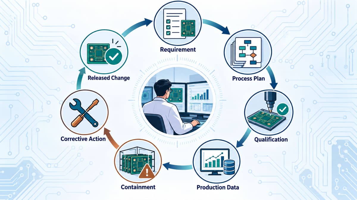
1. Translate requirements into measurable outputs. The engineer reviews the stack-up, finished thickness, copper requirement, minimum features, hole table, surface finish, impedance notes, and acceptance standard. Ambiguous notes are resolved before a recipe is selected. Otherwise, a line can produce internally consistent boards that still fail the customer’s requirement.
2. Select the route and define the process window. Material type, layer count, via structure, aspect ratio, copper build, and finish determine the route. The engineer identifies critical inputs and outputs rather than treating every setting as equally important. Limits must come from approved specifications, equipment capability, trials, and validated history—not a convenient nominal value.
3. Qualify the process. Trials establish whether the planned materials, tooling, equipment, inspection method, and operators can hold the requirement. Coupons, cross-sections, dimensional results, electrical tests, or other agreed evidence may be used. Passing one panel is not capability evidence; variation across the intended operating range has to be understood.
4. Release controlled instructions. The released route should identify revision, equipment or line, recipe, inspection points, sampling, reaction plan, and record owner. A verbal adjustment that is not reflected in controlled instructions creates an untraceable process change.
5. Monitor production data. Yield alone is a late indicator. Engineers watch measurable characteristics and trends: registration, etched feature results, hole condition, plating distribution, thickness, defect categories, rework, and test fallout as applicable. A value can remain inside a limit while its trend shows that the process is drifting.
6. Contain abnormal product. When a signal crosses a reaction limit, the first task is to define the affected time, equipment, lot, panel, and downstream inventory. Production material is separated before troubleshooting experiments begin. Without containment, good analysis may still allow questionable boards to ship.
7. Correct, verify, and release the change. Root-cause work distinguishes a symptom from the physical mechanism. The correction is tested, its side effects are checked, documents are updated, and affected personnel are trained. A changed recipe is not fully released until the resulting output is verified and traceable.
Which PCB Processes Need Direct Engineering Control?
Every step needs a defined owner, but the control mechanism changes with the physics of the process.
| Process area | What the engineer controls | Typical failure signal | Buyer evidence to request |
|---|---|---|---|
| Imaging and etching | Artwork compensation, exposure/development condition, etch balance, feature measurement | Necking, shorts, width drift, uneven copper removal | Feature inspection method and lot acceptance record |
| Lamination | Material lot, lay-up, press cycle, resin behavior, registration method | Voids, delamination, thickness or registration shift | Released stack-up and applicable coupon/cross-section evidence |
| Drilling and desmear | Tool choice/life, entry and backup, hit count, hole preparation | Smear, rough walls, breakout, oversized or undersized holes | Tool-control method and hole/cross-section results |
| Electroless copper and plating | Bath condition, current distribution, panel loading, thickness verification | Thin copper, nodules, voids, distribution problems | Plating records and agreed coupon measurements |
| Solder mask and finish | Registration, coating/cure, surface preparation, finish-specific controls | Mask encroachment, adhesion failure, poor surface condition | Visual criteria and finish verification documentation |
| Profiling and electrical test | Program revision, tooling, dimensional method, netlist/test release | Outline error, burrs, false pass/fail, wrong test program | Final inspection and electrical-test status by lot |
How Are Yield Problems Investigated?
A disciplined investigation begins with a defect definition that another person can reproduce. The team confirms the failure, maps it by lot/panel/location, checks when the signal changed, and compares affected material with known-good output. Only then should it rank possible causes and run controlled checks.
- Define: state the measured defect, requirement, sample identity, and detection stage.
- Contain: identify the last known-good point and hold the potentially affected scope.
- Stratify: compare machine, shift, material lot, panel position, tool, bath, and time.
- Verify the mechanism: use measurements or sections to show how the defect formed.
- Correct and challenge: test the proposed action under representative conditions.
- Prevent recurrence: update the control plan, instruction, limit, maintenance, or design feedback.
For example, intermittent plated-through-hole opens should not be closed as “plating variation” based on an electrical failure alone. Cross-sections and lot mapping may distinguish incomplete hole-wall preparation, local plating distribution, drilling damage, or test/contact error. Each cause requires a different correction.
Which Metrics Show Whether the Process Is Healthy?
First-pass yield is useful, but it can hide rework and mixed defect mechanisms. A better review combines output, variation, escape, and response metrics.
- First-pass and final yield by product family and process step
- Defect pareto with stable definitions and detection stage
- Critical-characteristic trends and capability where measurement systems are suitable
- Rework, scrap, retest, and false-call rates
- Containment response time and recurrence after corrective action
- Customer escapes linked back to lot, route, inspection, and change history
A high average yield does not prove that a demanding board is controlled. Buyers should ask whether results are separated by relevant technology and whether a process change can be linked to the affected lots.
What Skills and Tools Does the Role Require?
The role combines PCB process knowledge with experimental discipline. Useful tools include drawings and CAM data, measurement-system studies, control charts, designed trials, defect mapping, cross-section analysis, microscopy, chemical and equipment records, cause-and-effect analysis, and controlled change documentation. The engineer also needs to explain a finding in language that operators, designers, quality teams, and customers can act on.
Software does not replace judgment. A control chart cannot rescue an unreliable measurement, and a root-cause template cannot prove a mechanism. The engineer must know what was measured, how uncertainty affects the decision, and what evidence would disprove the favored explanation.
What Should Buyers Ask a PCB Manufacturer?
Ask for evidence that connects your board to the factory’s actual control system—not a generic equipment list.
- Who owns DFM questions, process release, deviations, and customer communication?
- Which characteristics are critical for this stack-up and via structure?
- How will the manufacturer qualify a non-routine material or process?
- What lot, panel, coupon, inspection, and electrical-test records are retrievable?
- What event stops production, and how is affected material contained?
- How are process, material, equipment, and supplier changes reviewed and communicated?
- What evidence will accompany first article, prototype, or production release?
The quality of the answers matters more than the number of certificates on a brochure. A credible response identifies the owner, the record, the decision limit, and the action when the result is abnormal.
Frequently Asked Questions
Is a PCB process engineer the same as a PCB designer?
No. A designer defines the electrical and physical product; a process engineer defines and controls how the factory produces it. They collaborate during DFM because design choices can narrow or destabilize the manufacturing window.
Does one engineer control the whole PCB factory?
Usually responsibility is divided by process family or technology, with cross-functional ownership for product release and failures. What matters is that each decision has an identified owner and escalation path.
What is the difference between process and quality engineering?
Process engineering controls how output is created; quality engineering governs conformance, systems, audits, and disposition. The exact boundary varies, so a supplier should explain it for your project.
Why is SPC not enough by itself?
SPC detects patterns only when the measurement and sampling plan are meaningful. It does not define the correct specification, prove a failure mechanism, or replace containment.
When is process qualification needed?
Qualification is appropriate for new or materially changed products, materials, equipment, routes, or operating windows according to the applicable quality system and customer agreement.
What evidence should accompany a prototype?
Agree this before ordering. Depending on risk, it may include stack-up confirmation, dimensional and electrical-test status, coupons, cross-sections, finish documentation, or a first-article package.
Can a high final yield still hide risk?
Yes. Heavy rework, repeated retest, mixed lots, or an unstable critical characteristic may still produce a high final pass rate. Review first-pass yield and the underlying defect and variation data.
What files help a process engineer review a quote?
Provide Gerber or ODB++ data, NC drill files, stack-up, fabrication drawing, material and finish requirements, impedance information, acceptance standard, quantity, and any special test or documentation needs.
Request a PCB Engineering Review
A capable process engineer should be able to explain how your critical requirements will be translated into controls, evidence, and a reaction plan. Send pcbtry your Gerber files, drill files, stack-up, fabrication drawing, material specification, quantity, and acceptance requirements through the contact or quotation channel. The engineering team can review manufacturability, identify open questions, and define the evidence needed before production.



0 Comments