




You can tell how many layers a PCB has by checking the board edge, copper plane clues, vias, routing density, light transmission, and design files. For a loose board, these checks can give a strong estimate, but they do not always prove the exact layer count. The reliable proof is the stackup drawing, Gerber layer set, drill files, or a manufacturer cross-section review.
This matters because layer count changes routing space, impedance control, board thickness, cost, lead time, and DFM risk. If you are preparing a quote or trying to identify an unknown board, use visual clues first, then confirm with files before making manufacturing decisions.

Start With What PCB Layer Count Means
PCB layer count means the number of conductive copper layers used inside the board. A 1 layer PCB has copper on one side. A 2 layer PCB has copper on both outer sides. A 4 layer PCB usually has two outer signal layers plus two internal planes or signal layers. Higher layer counts add more internal copper layers for dense routing, controlled impedance, power integrity, or compact designs.
Do not confuse layer count with board thickness, solder mask color, or how many components are mounted. A thick board can still be 2 layer, and a thin board can be 4 layer or more. The layer count is about copper structure, not only the outside appearance.
Check the Board Edge and Copper Planes
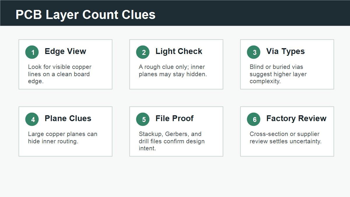
The board edge is often the first useful clue. On some boards, especially if the edge is cleanly routed or cut, you may see thin copper lines inside the laminate. These lines can suggest internal layers. Use a magnifier, side lighting, and a clean edge instead of judging from a damaged corner.
This clue is helpful but not perfect. Edge plating, copper pour, scoring marks, or dark FR-4 can hide or distort the view. If the edge suggests more than two copper layers, treat it as a reason to verify the stackup, not as final proof.
Use Light Only as a Rough Clue
Holding a PCB against strong light can sometimes help separate simple boards from more complex boards. A thin 2 layer board may let more light through. A multilayer board with inner planes may look darker because internal copper blocks the light.
Light testing is only a rough clue. Board color, laminate thickness, copper coverage, solder mask, and inner plane size all affect the result. A dark-looking board is not automatically 4 layer, and a board that passes some light is not automatically 2 layer.
Read Vias, Pads, and Routing Density
Via behavior gives stronger clues than color. If most traces visibly connect from top to bottom with standard through-hole vias, the board may be 2 layer. If the board has many dense BGA escape routes, hidden routing, blind vias, buried vias, or via-in-pad structures, it is likely to need more layers.
For high-density boards, vias are often used to move signals between internal layers. If you see technology such as blind and buried vias, review PCBTRY’s guide to blind and buried vias in PCBs because these features usually belong to more complex stackups.
Compare 2 Layer, 4 Layer, and 6 Layer Clues
The easiest way to judge an unknown board is to compare clues instead of looking for one magic sign. A 2 layer board usually has visible top and bottom routing. A 4 layer board often hides power and ground planes inside. A 6 layer or higher board usually appears in denser, higher-speed, impedance-controlled, or space-limited designs.
| Likely Layer Count | Common Clues | What to Verify |
| 1 layer | Copper only on one side, simple routing, low density | Single copper layer in files |
| 2 layer | Top and bottom traces, standard through vias, simpler layout | Top copper, bottom copper, drill file |
| 4 layer | Inner plane clues, darker light result, denser routing, cleaner outer layers | Stackup drawing and internal Gerbers |
| 6 layer or more | High density, controlled impedance, BGA escape, blind/buried vias possible | Complete stackup, impedance notes, drill structure |
If you are still learning the difference between board structure and layout work, PCBTRY’s article on what a PCB is and what PCB design means gives helpful context.
When You Cannot Confirm Layer Count by Eye
You cannot always confirm PCB layer count by eye. A board may have internal copper planes that are not visible from the outside. A dense 2 layer board can look complex, while a well-designed 4 layer board can look visually clean. Some boards also hide clues under solder mask, components, conformal coating, or dark laminate.
When the answer affects ordering, redesign, repair, or quotation, do not rely only on appearance. Ask for the fabrication files or request a manufacturer review. For critical boards, cross-section inspection can physically show the internal copper structure.
What Files Prove PCB Layer Count
The most reliable proof is the file package. The stackup drawing states the layer order, dielectric thickness, copper weight, and sometimes impedance rules. Gerber files show the copper layers. Drill files show via structure. Fabrication notes explain plated holes, controlled impedance, blind vias, and special requirements.
Before quoting, prepare Gerbers, drill files, board thickness, copper weight, surface finish, material requirements, and any impedance notes. If the board uses HDI features, PCBTRY’s HDI PCB design guide can help you understand why stackup confirmation becomes more important.
Why Layer Count Changes Cost, Thickness, and DFM
Layer count changes the manufacturing process. More layers usually mean more lamination steps, tighter registration, more process control, and more stackup planning. This can affect cost, lead time, yield risk, impedance control, and DFM review.
A 4 layer board is not just a 2 layer board with extra copper. The designer must decide how power, ground, signals, thickness, material, vias, and impedance work together. For manufacturability planning, review PCBTRY’s DFM and DFA in PCB manufacturing guide before finalizing the stackup.
Layer Count Checklist Before Quotation
Use this checklist before sending an unknown or new PCB for quotation.
- Check the board edge for visible internal copper lines.
- Use light only as a rough clue, not final proof.
- Inspect via types, routing density, BGA areas, and plane clues.
- Compare visible clues with expected 2 layer, 4 layer, or 6 layer behavior.
- Collect Gerbers, drill files, stackup drawing, board thickness, copper weight, and material notes.
- Mark controlled impedance, blind vias, buried vias, or HDI requirements clearly.
- Ask the manufacturer to verify layer count before pricing or rebuilding the board.
- For critical boards, request cross-section or engineering review instead of guessing.
FAQs About Telling How Many Layers a PCB Has
Can I tell PCB layer count just by looking at the board?
Sometimes you can estimate it, but you cannot always prove it. Edge view, vias, and routing clues help, while stackup files or cross-section review give stronger confirmation.
Does a dark PCB mean it has more layers?
Not always. A board may look dark because of solder mask, laminate, thickness, or copper coverage. Darkness is only a clue, not proof.
Can I use a flashlight to identify a 2 layer PCB?
A flashlight can help as a rough test. If light passes through easily, the board may be simpler, but inner copper planes, board thickness, and material can change the result.
How can I tell if a PCB is 2 layer or 4 layer?
Look for internal copper at the edge, cleaner outer routing, plane behavior, via density, and design files. A 4 layer board often hides power and ground planes inside.
Do blind vias mean the PCB has more than 2 layers?
Usually yes. Blind and buried vias are used to connect selected layers and normally require a multilayer stackup.
What file shows PCB layer count most clearly?
The stackup drawing is usually the clearest file. Gerber layer files and drill files also help prove the copper layer structure.
Why does the manufacturer need layer count for a quote?
Layer count affects lamination, material, copper, drilling, registration, testing, lead time, and cost. Wrong layer count can make the quote inaccurate.
Can PCBTRY help confirm an unknown board layer count?
Yes. Send Gerbers, drill files, stackup notes, photos, board thickness, quantity, and special requirements to [email protected] for engineering review.
Is a multilayer PCB always better than a 2 layer PCB?
No. More layers can improve routing, EMI control, and power integrity, but they also add cost and process requirements. The right choice depends on the circuit.
Send PCB Stackup Files for Review
If you need to confirm PCB layer count before quotation, rebuilding, or manufacturing, send Gerbers, drill files, stackup drawing, board thickness, copper weight, photos, quantity, and any impedance or HDI requirements to [email protected]. PCBTRY can review the layer structure and manufacturing risks before production.



0 Comments