




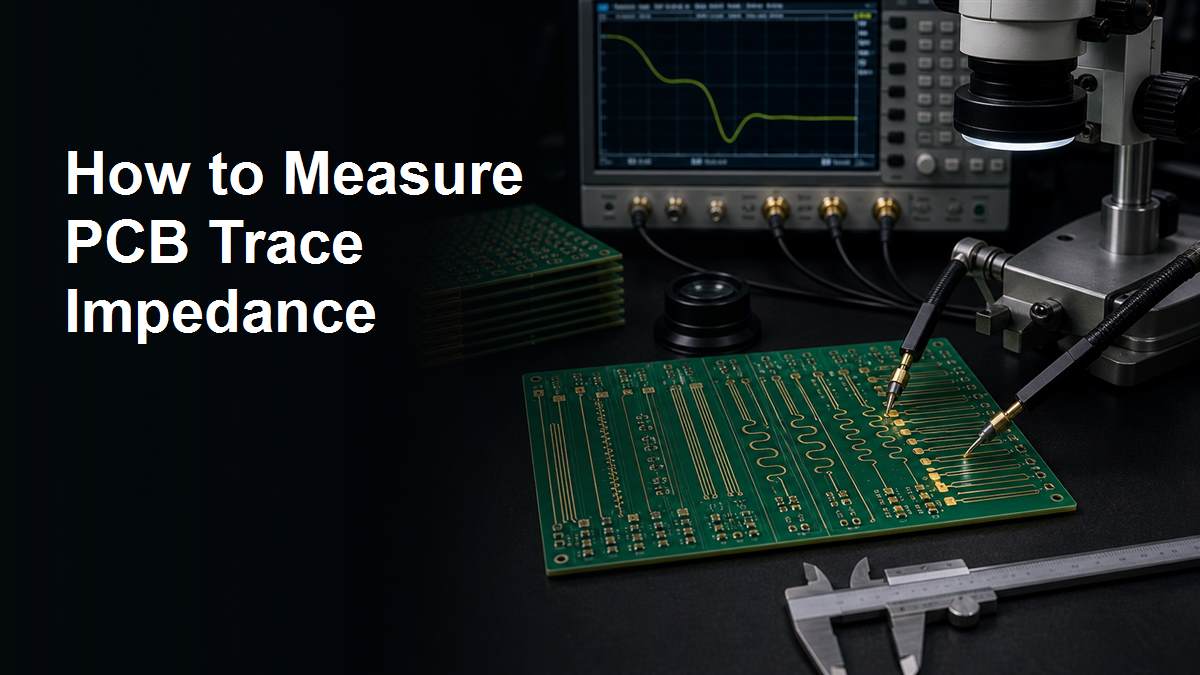
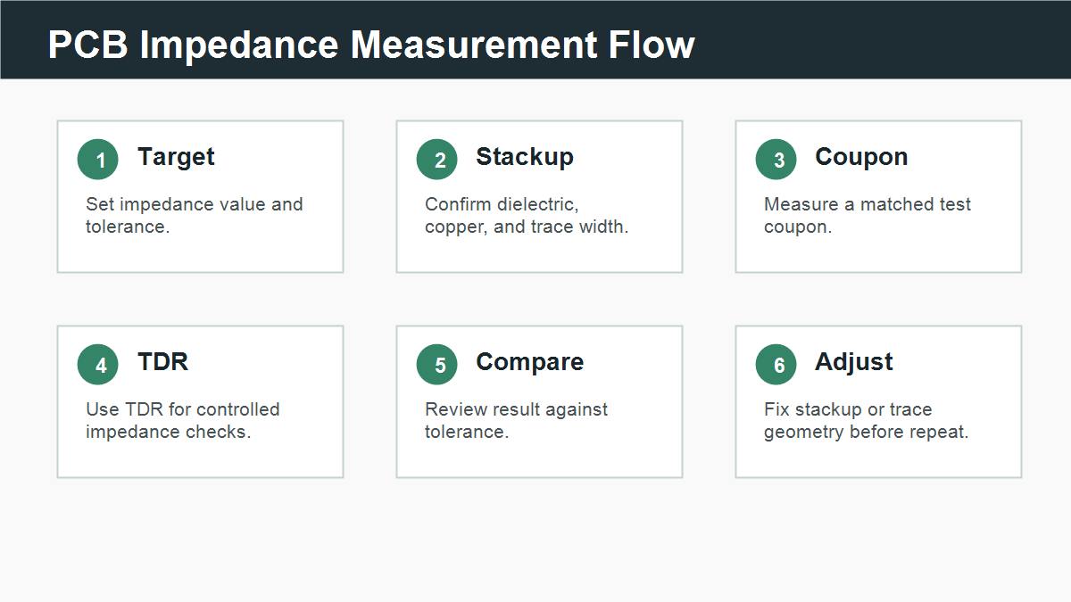
To measure PCB trace impedance, use a controlled impedance test method such as TDR on a test coupon or a designed measurement structure. A normal multimeter cannot measure characteristic impedance because impedance depends on trace geometry, dielectric thickness, dielectric constant, copper thickness, reference plane, and signal behavior at high frequency. For manufacturing control, the impedance target must be defined in the stackup and checked against a tolerance after fabrication.
This guide explains what can be measured, what cannot be measured with simple tools, and what files to send when you need controlled impedance review before PCB production.
Start With What Trace Impedance Means
PCB trace impedance is the opposition a high-speed signal sees as it travels along a trace. It is not the same as DC resistance. A trace can have very low resistance but still have the wrong impedance for USB, Ethernet, RF, DDR, LVDS, or other controlled signals.
The value depends on trace width, copper thickness, dielectric height, dielectric constant, solder mask, reference plane, and whether the trace is single-ended or differential. This is why impedance must be planned with the stackup, not guessed after routing.
Do Not Use a Multimeter to Measure Characteristic Impedance
A multimeter can check continuity, opens, shorts, and sometimes low resistance, but it cannot measure characteristic impedance. If you touch meter probes to a PCB trace, you are measuring a DC condition, not the high-frequency transmission-line behavior.
This matters because a board may pass continuity testing and still fail signal integrity. If the design needs a 50 ohm single-ended trace or 90 ohm differential pair, use stackup calculation before fabrication and TDR-style verification after fabrication.
Use TDR or a Controlled Test Coupon
TDR, or time-domain reflectometry, sends a fast signal into the trace and reads reflections caused by impedance changes. In production, the manufacturer often measures an impedance test coupon placed on the same panel as the real PCB. The coupon uses the same stackup and trace geometry as the board.
A coupon is easier and safer to test than probing a finished product trace, especially when components, connectors, solder mask, or access limits make direct probing difficult. For PCBTRY production review, include impedance requirements before manufacturing instead of asking for measurement only after boards are built.
Measure Coupon Results Against a Tolerance
Impedance measurement is not just a yes-or-no check. The result must be compared with the required tolerance. Common projects may use a tolerance such as plus or minus 10 percent, but the exact requirement depends on the design and should be confirmed in the fabrication notes.
If results are outside tolerance, the cause may be trace width, dielectric thickness, material Dk, copper thickness, etching variation, reference plane distance, or incorrect coupon design. Do not change only one number without reviewing the whole stackup.
Know When to Measure on the Board Itself
Sometimes engineers measure a trace on the finished board, especially for failure analysis, RF tuning, or prototype validation. This requires suitable access points, fixtures, probes, calibration, and knowledge of connectors and stubs.
Board-level measurement is more complex than coupon testing. It can be affected by components, vias, connectors, solder joints, and probe launch quality. For manufacturing acceptance, coupon measurement is usually the cleaner evidence.
Prepare Stackup and Trace Data Before Fabrication
Controlled impedance should be designed before PCB fabrication. Send the target impedance, tolerance, layer name, trace width, spacing for differential pairs, reference plane, copper weight, material, board thickness, and stackup drawing. If you are still defining the board structure, PCBTRY’s guide on how to tell how many layers a PCB has helps explain why layer structure matters.
For HDI or dense routing, impedance and via structure should be reviewed together. PCBTRY’s HDI PCB design guide is useful when microvias, fine traces, or compact stackups are involved.
Check Vias, Stubs, and Reference Planes
Even if a straight trace is correct, vias and reference plane changes can disturb impedance. A via can add inductance and capacitance. A long unused via stub can create reflection. A missing return path can create noise and signal integrity problems.
If your controlled impedance route changes layers, check the via type, return via, reference plane continuity, and trace geometry after the layer transition. For via planning, review PCBTRY’s how to make vias on PCB guide.
PCB Trace Impedance Measurement Checklist
Use this checklist before asking for controlled impedance production or measurement.
- Target impedance and tolerance are defined.
- Single-ended or differential impedance is clearly stated.
- Layer name, trace width, and differential spacing are listed.
- Stackup, dielectric thickness, material, copper weight, and board thickness are included.
- Reference plane and return path are checked.
- Vias, stubs, connectors, and layer transitions are reviewed.
- Test coupon requirement is confirmed with the manufacturer.
- TDR report or measurement requirement is requested before production approval.
FAQs About Measuring PCB Trace Impedance
Can I measure PCB trace impedance with a multimeter?
No. A multimeter measures DC continuity or resistance, not characteristic impedance.
What tool is used to measure PCB impedance?
TDR is commonly used for controlled impedance coupon measurement. Some RF work may also use VNA methods with proper fixtures.
What is an impedance test coupon?
It is a small test structure fabricated on the same panel as the PCB, using matched stackup and trace geometry for measurement.
Should I measure the coupon or the actual trace?
For manufacturing acceptance, coupon measurement is usually cleaner. Board traces may be measured for prototype validation or troubleshooting.
What files are needed for impedance control?
Send Gerbers, drill files, stackup drawing, impedance target, tolerance, layer, trace width, spacing, copper weight, and material notes.
Why can impedance be wrong if the trace width is correct?
Dielectric thickness, Dk, copper thickness, etching, solder mask, and reference plane distance also affect impedance.
Does every PCB need impedance control?
No. It is mainly needed for high-speed, RF, differential, or timing-sensitive signals.
Can PCBTRY provide impedance testing?
Send your stackup, Gerbers, impedance table, coupon needs, quantity, and tolerance notes to [email protected] for review.
When should impedance be discussed with the manufacturer?
Before fabrication, because stackup and trace geometry may need adjustment before the board is built.
Send Controlled Impedance Files for Review
If your PCB needs controlled impedance, send Gerbers, drill files, stackup drawing, impedance table, target tolerance, material notes, copper weight, board thickness, quantity, and coupon requirements to [email protected]. PCBTRY can review manufacturability and measurement requirements before production.



0 Comments