




What It Means to Trace a PCB Circuit
To trace a PCB circuit means to find which pads, pins, traces and components are electrically connected on a printed circuit board. You may do this because the schematic is missing, a board is damaged, a signal is not reaching the next component, or you need to remake an old PCB from the physical sample.
In plain language, you are building a map. A PCB can look like a flat green board, but electrically it is a network of copper paths. Some paths are visible on the top or bottom layer. Some disappear through vias to another layer. Some seem connected because a component sits between them, but they are not the same net.
The goal is not to guess where the trace goes. The goal is to prove the path with visual inspection, continuity checks, component understanding and notes that another engineer or PCB manufacturer can use.
Start With Safety and Board Condition
Do not trace a powered board unless you are specifically doing live voltage measurements and know the risk. For normal continuity tracing, the board should be unpowered and discharged. Capacitors can hold charge, and some boards connect to mains or high voltage supplies.
Before using a meter, inspect the board. Look for burnt areas, cracked solder joints, lifted pads, corrosion, missing components, scraped solder mask and broken traces. A damaged board may give confusing readings because copper is partly cracked or contaminated.
If the board is dirty or corroded, clean only when you know the residue type and component sensitivity. A wet or contaminated board can create leakage paths that make continuity results unreliable. For heavy corrosion, record photos before cleaning so the original trace evidence is not lost.
Tools You Need to Trace PCB Tracks
You can start with simple tools. A bright light, magnifier, phone camera, fine marker, multimeter and printed board photo are enough for many two-layer boards. For complex boards, you may need microscope inspection, board scans, X-ray, schematic comparison or layout reconstruction.
| Tool | Use | Limit |
|---|---|---|
| Bright light and magnifier | Follow visible copper, vias and pad shapes | Cannot see inner layers |
| Multimeter continuity mode | Checks whether two exposed points are connected | Can be fooled by components or parallel paths |
| Ohms mode | Shows resistance instead of only a beep | Still affected by in-circuit parts |
| Board photo or scan | Lets you mark nets without writing on the board | Needs good angle and lighting |
| Schematic or datasheet | Confirms pin functions and expected nets | May not match an unknown or revised board |
Identify the Component Pins and Reference Points
Start from something known. It might be a connector pin, IC pin 1, ground pad, power input, test point or component reference. If you begin from a random copper line, you may trace the wrong part of the circuit and waste time.
Use component markings and datasheets when possible. For an IC, identify pin 1 and the package orientation. For a connector, confirm whether you are looking from the top side, bottom side or cable side. Mirrored connector views are a common source of wrong tracing notes.
Mark ground first. Ground usually connects to mounting holes, shield cans, large copper pours, negative capacitor terminals or connector shells, but do not assume. Prove it with continuity and visual evidence.
Follow Visible Traces Before Using the Meter
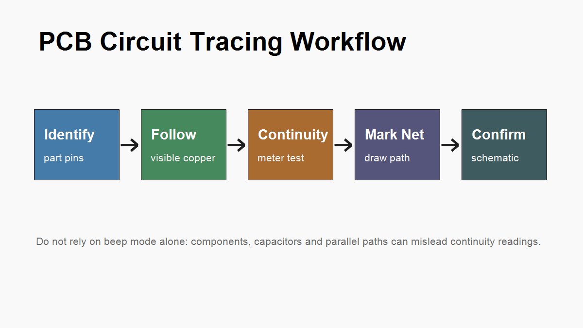
Use your eyes first. Visible tracing teaches you the physical route: which pad leaves the component, where the trace narrows, whether it goes through a via, and where it appears again. This prevents blind meter probing.
Good lighting helps. Tilt the board so copper edges and solder mask thickness become visible. Take a high-resolution photo and mark the path digitally. If the board has both sides populated, photograph both sides in the same orientation so vias can be matched more easily.
When a trace disappears into a via, mark the via number or location, then check the other side. On multilayer boards, the via may connect to an inner layer, so a visible route may stop. That is when continuity testing and schematic logic become more important.
Use Continuity Mode Correctly
Continuity mode is useful, but it is not magic. A beep usually means the meter sees a low-resistance path between the probes. It does not always mean the two points are directly connected by one copper trace.
Components can create paths. Inductors, coils, transformers, low-value resistors, fuses and solder bridges may beep. Capacitors may beep briefly while charging. Semiconductor junctions can show confusing readings depending on polarity and meter voltage.
The safer method is to combine beep mode with resistance mode. If two pads beep and measure near zero ohms, they are likely the same net. If they beep weakly, change over time or show several ohms through a component, treat the result as a clue, not a final conclusion.
| Reading | Likely meaning | Next check |
|---|---|---|
| Strong beep, near 0 ohms | Same copper net or very low resistance path | Confirm visually if possible |
| Brief beep then stops | Capacitor charging or transient path | Reverse probes and use resistance mode |
| Beep through a coil or fuse | Component path, not same copper trace | Identify component and mark separately |
| No beep but expected connection | Broken trace, via fault, switch/contact, high resistance path | Check nearby points along the route |
| Beep across power and ground | Possible short or low-resistance load | Do not power up before diagnosis |
Build a Net Map as You Trace
A net map is a record of which points are electrically connected. It can be a marked-up photo, spreadsheet or hand drawing. The important part is consistency. Give each confirmed net a name, such as GND, VIN, 5V, RESET, LED_A or U1 pin 3 net.
Mark confirmed connections differently from suspected connections. For example, use a solid line for proven continuity and a dotted line for a visually suspected route. Add notes when a path goes through a resistor, diode, coil or connector rather than direct copper.
This record is what turns tracing into useful engineering work. Without notes, you may know the answer for five minutes and then lose it. With notes, you can compare the board to a schematic, repair a broken trace or prepare a replacement PCB.
Trace Through Vias, Pads and Hidden Layers
Vias are small plated holes that carry a signal from one layer to another. On a simple two-layer board, a via often lets you follow a trace from top to bottom. On a multilayer board, the route may move into an internal layer that you cannot see.
Probe exposed vias carefully. If the via is covered by solder mask, do not scrape aggressively unless repair is already planned. Damaging the mask or copper can create a new fault. Look for test pads, connector pins or component pads on the same net before scraping.
If several vias connect to the same plane, such as ground or power, continuity may show many points connected. That is normal. The task is to separate plane connections from signal traces. Large copper pours, thermal reliefs and many repeated via connections often indicate a plane rather than one narrow signal route.
Find Broken Traces or Suspect Connections
To find a broken PCB trace, test in small sections instead of jumping from one end of the circuit to the other. Start at a known pad and move along the visible route, probing at vias, exposed pads or component leads. The break is usually between the last point that connects and the first point that does not.
Common break points include connector pads, flexing areas, burnt spots, corroded regions, scraped solder mask, thin neck-down traces and vias near mechanical stress. If the board has been dropped or repaired before, check around heavy parts and connectors first.
Once you find a likely break, do not immediately add a jumper without understanding the net. Confirm that the broken path is not intentionally isolated by a resistor, fuse, switch, zero-ohm link or configuration option. A wrong jumper can create a short or bypass a protection component.
Know When Tracing Is Not Enough
Tracing tells you connectivity. It does not fully tell you signal quality, impedance, current capacity, insulation safety or firmware behavior. A traced connection can still fail under load, at high frequency or during temperature changes.
If the circuit involves RF, high-speed digital signals, high voltage, power conversion, fine-pitch BGAs or controlled impedance, visual tracing and continuity checks are only a first step. You may need schematic reconstruction, layer stackup review, X-ray, impedance measurement or professional failure analysis.
For a board that must be remade, tracing should become a controlled design package. PCBtry can help review manufacturing files for PCB fabrication, but an unknown board may first need schematic capture and layout reconstruction before it is safe to fabricate.
Prepare Repair or Remake Notes
If your goal is repair, record the fault location, confirmed net, suspected cause and intended jumper or pad repair. If your goal is remaking the PCB, record more: component locations, connector orientation, mounting holes, board thickness, copper weight, layer estimate, surface finish, solder mask color and any missing schematic information.
Photos are especially useful. Take one clean photo before repair, one with marked nets, and one after any jumper or trace repair. If you need manufacturing help, send these with your Gerber files, schematic, board photos and target quantity through PCBtry contact.
PCB Circuit Tracing Checklist
Use this checklist before you trust your tracing result:
- The board is unpowered and discharged for continuity tracing.
- Connector orientation and pin 1 are confirmed.
- Ground and power nets are identified separately.
- Visible traces are followed before random probing.
- Continuity readings are checked with resistance mode when unclear.
- Components that create paths are marked, not mistaken for copper traces.
- Vias and hidden-layer uncertainty are recorded.
- Broken trace repair is confirmed before adding jumpers.
- Photos and net notes are saved for repair, remake or fabrication review.
FAQs About How to Trace PCB Circuit
Can I trace a PCB circuit without a schematic?
Yes, especially on simple one-layer or two-layer boards. For multilayer or dense boards, you can trace some nets, but a full schematic may require deeper reverse engineering.
Does continuity beep mean two points are the same trace?
Not always. A beep can pass through coils, fuses, low-value resistors or other components. Use resistance readings and visual evidence before calling it the same net.
How do I trace a PCB circuit on a multilayer board?
Start with visible pads, vias and known components, then build a net map. Hidden layers may require schematic data, X-ray, layout files or professional analysis.
What should I do if I find a broken PCB trace?
Confirm both sides of the break, identify the net, check whether a component should be in the path, then plan a controlled jumper or pad repair.
Can I scrape solder mask to test a trace?
Only when necessary and carefully. It is better to use exposed pads, vias, test points or component leads first because scraping can damage copper.
Why does my meter show continuity across power and ground?
It may indicate a short, but it can also be a low-resistance load or capacitor behavior. Do not power the board until you understand the reading.
Can PCBtry make a new PCB from a traced board?
PCBtry can manufacture from proper production files. If you only have a traced physical board, prepare schematic, layout or reconstruction files first, then submit Gerber, drill and fabrication notes for review.
What files help when asking for repair or remake advice?
Send clear board photos, marked net notes, schematic if available, Gerber files if available, fault description, board dimensions, layer estimate and target quantity.



1 Comment
How to Cross-Check a PCB Schematic Against the Physical Board - thindry pcb manufacturer · 08/26/2026 at 08:28
[…] How to Trace a PCB Circuit for repair-oriented tracing and continuity checks. […]