Blog
Bare PCB Manufacturing Process: Fabrication Steps, Controls and Final Testing
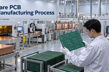
See how bare PCBs move from CAM review through imaging, lamination, drilling, plating, finishing, inspection and electrical testing.



See how bare PCBs move from CAM review through imaging, lamination, drilling, plating, finishing, inspection and electrical testing.
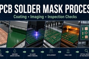
See how PCB solder mask is prepared, coated, imaged, developed, cured and inspected for registration, coverage and adhesion defects.
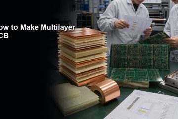
See how multilayer PCBs are designed, imaged, laminated, drilled, plated, finished, and tested, plus the files and DFM checks needed before fabrication.
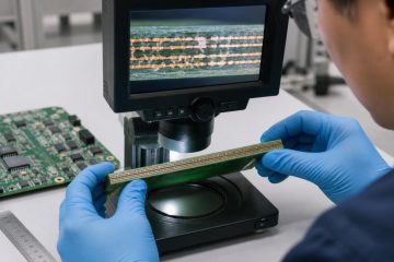
Learn how to identify PCB copper layers using design files, board-edge clues, vias, X-ray, and cross-section evidence, with clear limits for each method.
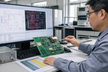
Evaluate a China PCB design service by defining inputs, stackup, DFM, review milestones, source-file ownership, and the final manufacturing handoff.
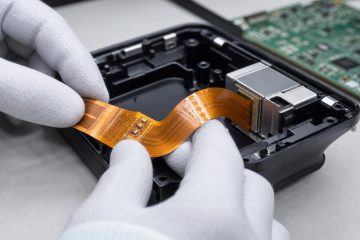
Learn how to make a flexible PCB by choosing the right stackup, protecting bend areas, preparing fabrication files, and checking the finished flex circuit.
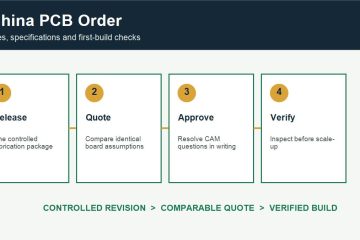
Prepare a China PCB order with practical checks for fabrication files, board specifications, quote assumptions, CAM questions and first-build inspection.
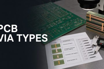
Learn the main PCB via types, how through vias, blind vias, buried vias, microvias and via-in-pad differ, and what to check before fabrication.
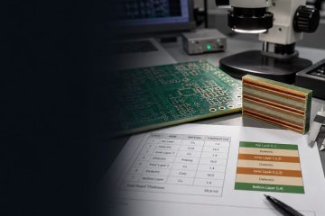
Learn a practical 4 layer PCB stackup, when to use signal-ground-power-signal layers, what to check for impedance, copper balance, vias and fabrication.
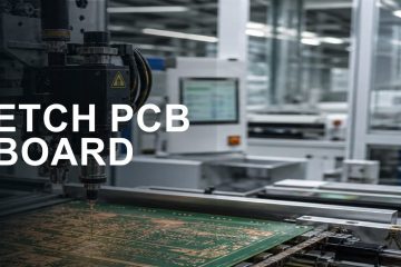
Learn how to etch a PCB board safely, from copper cleaning and resist transfer to etching checks, common failures and when to use factory fabrication.
If you have any enquiry about quotation or cooperation, please feel free to email us at [email protected] or use the following enquiry form. Oursales representative will contact you within 24 hours. Thank you for your interest in our products.