




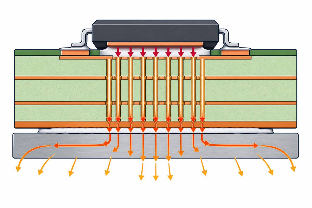
A component does not simply release heat into open air. Heat must travel from the semiconductor junction or resistive element through the package, solder connection, PCB copper, vias, thermal interface, enclosure, heat sink, or surrounding air. PCB layout determines how continuous—or restrictive—that path becomes.
Two boards using the same component can therefore run at different temperatures. Texas Instruments notes that PCB design can dominate thermal performance for many medium-power parts; demanding systems may require modeling or prototype measurement.
For each major source, estimate realistic loss, identify the package-to-board conduction path, and define where the heat is finally rejected: air, enclosure, cold plate, or another sink.
If any link in that chain is missing, adding more copper or more vias may only move the hot spot rather than solve the thermal problem.
How Does Part Placement Shape PCB Hot Spots?
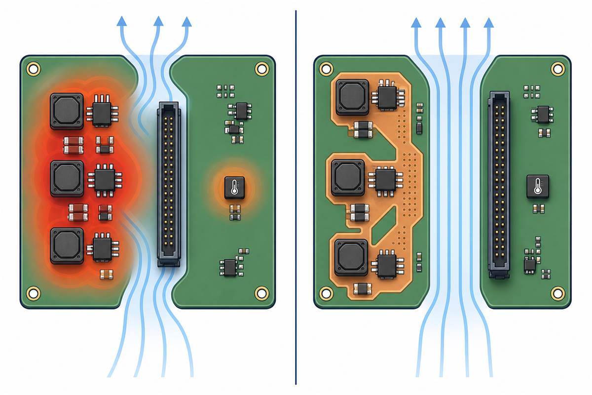
Placement establishes the thermal map before routing. Clustered high-loss components share the same copper and airflow region, which can create a local hot spot. Estimate realistic losses for major sources, then place them according to the available thermal path:
- Keep a high-dissipation package close to the copper area, chassis contact, or heat sink intended to receive its heat.
- Avoid placing tall components where they block airflow to a hot package or heat sink.
- Do not concentrate unrelated heat sources unless the cooling structure is designed for their combined load.
Placement is not independent of electrical performance. A switching regulator still needs short high-current loops and correct placement of its capacitors, inductor, and switching nodes, so the thermal plan must work inside those constraints.
If you are building placement skills, the PCBtry guide on how to learn PCB layout provides broader context for placement, routing, and design review.
How Do Copper Loss, Planes, and Stackup Affect Board Temperature?
Copper influences temperature in two different ways. First, current flowing through a resistive trace generates heat. Shorter, wider, or thicker conductors can reduce resistance when the electrical and manufacturing design permits. Second, connected copper can spread heat away from a component pad over a larger board area.
A wide power path can reduce trace loss, while a separate plane may mainly spread existing heat. Copper must remain continuous toward a cooler region; neck-downs, voids, splits, and isolated islands can interrupt the path.
More copper is not automatically better everywhere. Analog Devices shows an important power-layout trade-off: increasing copper on DC power and ground nodes can help heat spreading, but enlarging a high-dv/dt switch node may worsen noise and coupling. Thermal changes must therefore be reviewed with EMI and signal-integrity requirements.
When Do Thermal Vias and Exposed Pads Improve Heat Transfer?
Thermal vias can connect an exposed pad to internal or bottom copper, but their count and geometry are not universal. Begin with the component data sheet and package guidance because pad size, net, loss, board thickness, via process, and assembly differ.
Before placing a via array, confirm:
- The exposed pad’s required electrical connection and destination copper.
- Whether vias require filling, capping, plugging, or tenting.
- How holes, paste apertures, and plane connections affect soldering, voiding, and inspection.
Thermal-relief spokes reduce heat flow during soldering but can also restrict operating conduction. Use a solid connection only where package guidance and the assembly process support it.
Dense boards add routing and fabrication constraints. The PCBtry HDI PCB design guide can help readers place thermal decisions within the wider context of high-density stackups and microvia planning.
Published Engineering Scenario: Exposed-Pad Layout Sensitivity
Texas Instruments’ AN-1520 documents the LM2652 in a 28-lead exposed-pad TSSOP on five 3 × 3 inch, four-layer PCB layouts with different ground-plane arrangements.
Within that defined study, the revised board layouts reduced the reported junction-to-ambient thermal resistance from roughly 40–50°C/W to roughly 25–30°C/W. TI also examined ground-plane geometry, airflow, device power, solder coverage, thermal-via diameter, and via distribution.
The result shows layout sensitivity, not a universal improvement promise. Other boards require their own device data, loss, stackup, airflow, enclosure, and validation.
How Should the PCB Connect to Airflow, Heat Sinks, and the Enclosure?
The PCB is normally one part of the product’s cooling system. Copper and vias can move and spread heat, but the final temperature also depends on airflow, enclosure surfaces, board orientation, heat-sink geometry, interface materials, and ambient conditions.
For forced air, check whether connectors, shields, cables, or tall capacitors create an airflow shadow. For natural convection, check board orientation and vent position. For conduction cooling, align hot components with mounting points, gap pads, cold plates, or chassis regions. Contact area, pressure, isolation, interface thickness, and assembly tolerance belong in the model.
When reviewing an unfamiliar assembly, the guide on how to read and understand a PCB board explains how to recognize thermal vias, copper areas, heat sinks, and related board features.
How Should Heat-Sensitive Components Be Placed?
Good thermal management protects vulnerable components as well as cooling the hottest device. Temperature sensors, voltage references, precision analog circuits, oscillators, electrolytic capacitors, connectors, batteries, and some optoelectronic devices can be affected by local temperature or repeated thermal cycling.
Do not apply a universal separation distance. Compare the local environment with the part’s data-sheet limits, accuracy requirements, life target, and derating policy. Physical distance is not enough: a shared plane can conduct heat to a remote part. An ambient sensor should be isolated from unintended local heating, while a device-monitoring sensor needs deliberate, repeatable coupling.
Repeated hot and cold cycles can stress solder joints, vias, copper, laminate, and packages. For more context, see PCBtry’s article on what affects PCB durability over time.
Which Thermal Layout Trade-Offs Matter?
Review every thermal change across electrical, mechanical, fabrication, and assembly requirements.
| Proposed change | Possible thermal benefit | Trade-offs to review |
|---|---|---|
| Increase copper around a power device | Lower conductor loss or better spreading | Switch-node capacitance, EMI, routing congestion, creepage, copper balance |
| Add more thermal vias | Lower through-board path resistance | Routing area, drill capability, plane voiding, cost, diminishing benefit, assembly process |
| Use via-in-pad | Direct path below an exposed pad | Filling/capping requirements, solder wicking, voids, flatness, inspection, price |
| Use a solid plane connection | Improved operating heat conduction | Hand soldering, rework, through-hole solder fill, assembly profile |
| Move a hot component to a board edge | Potentially better chassis or airflow access | Electrical-loop length, connectors, mechanical stress, service access |
Confirm non-standard vias, heavy copper, metal-backed boards, embedded copper, and special interfaces with the fabricator before release.
How Can You Validate PCB Thermal Management Before Release?
Thermal rules are screening tools, not proof. Validation needs defined boundaries and evidence that temperatures meet the intended limits.
- Estimate realistic loss. Include the relevant conduction, switching, magnetic, and resistive losses at the intended operating point.
- Define boundaries. Record ambient, airflow, orientation, enclosure, neighboring sources, duty cycle, and worst-case load.
- Model appropriately. Use early calculations for screening and electrothermal or CFD analysis when interactions and margins require it.
- Estimate junction temperature correctly. Use package metrics that match the applicable test condition rather than treating one catalog value as universal.
- Measure prototypes. Document the method, location, emissivity or contact treatment, instrument accuracy, load, ambient, and stabilization time.
- Apply acceptance criteria. Check limits, margin, derating, touch temperature, materials, and reliability goals.
If measurement and model disagree, check loss estimates, contact resistance, airflow leakage, fixtures, cables, and measurement error.
PCB Thermal Layout Release Check
- Identify realistic losses and a continuous path from every major source to a defined sink.
- Check high-current copper, thermal pads, via arrays, and destination planes against component guidance.
- Review via processing, soldering, inspection, rework, and special fabrication requirements.
- Protect sensitive parts and confirm the real enclosure, airflow, orientation, and contact interfaces.
- Recheck electrical and mechanical constraints, then validate under documented worst-case conditions.
PCB Layout and Heat Dissipation FAQs
Does a four-layer PCB always dissipate heat better than a two-layer PCB?
No. Additional copper layers can create more spreading paths, but performance depends on copper continuity, layer spacing, via connections, board size, airflow, enclosure, and component power. A poorly connected multilayer board can still trap heat near the source.
Should every hot PCB component be placed near the board edge?
No. An edge can help when it provides airflow or a chassis interface, but moving the part may lengthen critical power loops, interfere with connectors, or create mechanical constraints. Placement must satisfy both the electrical circuit and the intended cooling path.
Do more thermal vias always reduce component temperature?
No. Vias need a useful copper plane, backside spreader, heat sink, or chassis path. Benefits can diminish as vias become crowded, and extra holes may disrupt lateral copper spreading or complicate assembly. Use package guidance and validate the complete path.
Can a ground plane be used as a PCB heat spreader?
Often, yes, when the component’s thermal pad is allowed to connect to ground and the plane is continuous. Verify the electrical net, package instructions, plane geometry, and where the plane releases the heat.
Are thermal-relief spokes good for heat dissipation during operation?
Thermal-relief spokes are mainly used to limit heat flow during soldering. They can restrict operating heat conduction compared with a solid connection. Use the pad and package manufacturer’s layout recommendation and coordinate with the assembly process.
Does thicker copper solve PCB overheating?
Not by itself. Thicker copper may reduce high-current conductor loss and improve spreading, but it cannot correct excessive component loss, a missing via path, poor airflow, a restrictive enclosure, or an inadequate heat-sink interface.
How should temperature sensors be placed near heat-generating parts?
First define what the sensor must measure. A device-monitoring sensor needs controlled coupling to the target, while an ambient sensor should be isolated from local copper and airflow disturbances. Validate its reading against a reference under realistic operating conditions.
When is PCB thermal simulation necessary?
Simulation becomes more valuable when power density is high, airflow or enclosure paths are complex, margins are small, several heat sources interact, or prototype iteration is expensive. The model still requires credible power, material, interface, and boundary-condition inputs.
How can thermal imaging mislead a PCB investigation?
Different surface emissivities, reflections from metal, viewing angle, focus, airflow changes, and insufficient stabilization can distort apparent temperature. Document the setup and use contact or electrical methods where a reliable junction estimate is required.
What information should a PCB manufacturer receive for a thermal review?
Provide the board files, stackup, copper requirements, component thermal-pad details, via construction, fill or cap requirements, expected power/load conditions, assembly process, heat-sink or enclosure interface, and any controlled acceptance criteria. The manufacturer can then assess fabrication and assembly feasibility; system thermal performance still requires design validation.
Plan a Manufacturable PCB Thermal Path With PCBtry
For a quotation or DFM review, provide Gerber or ODB++ data, drill files, stackup, copper requirements, pad/via details, component documents, assembly constraints, and the intended heat-sink or chassis interface. Confirm final thermal performance with component data, appropriate modeling, and prototype measurements.



2 Comments
AI for PCB Layout: What It Can Automate and How to Verify Results - thindry pcb manufacturer · 08/26/2026 at 08:29
[…] PCB thermal-path analysis and temperature validation; […]
A4988 PCB Layout Guide: Placement, Routing, Grounding and Thermal Checks - thindry pcb manufacturer · 08/26/2026 at 08:31
[…] across realistic voltage, motion, ambient, enclosure, and airflow. PCBtry’s discussion of how PCB layout changes the heat path can help structure that […]