




How Do You Drill a PCB Without Damaging It?
To drill a PCB cleanly, first decide whether the job is a simple hole in an unpopulated DIY board or a production hole that must be plated, aligned across layers, or held to a controlled tolerance. For a simple board, use a rigid high-speed rotary tool or drill press, a sharp carbide PCB bit, firm backing material, and light vertical feed. For plated through-holes, multilayer vias, dense layouts, or quantity production, send accurate drill data to the fabricator instead of drilling the finished board by hand.
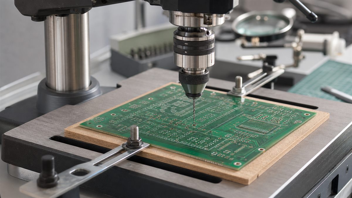
The practical sequence is: confirm the hole function, select the finished size, choose the correct tool diameter, support and clamp the board, drill perpendicular to the surface, clean the debris, then inspect position, edge quality, copper clearance, and fit. A hole that merely looks round is not automatically acceptable.
Should You Drill the PCB by Hand or Let the Factory Drill It?
Hand drilling is reasonable for a low-risk prototype, an unplated single- or double-sided DIY board, or a noncritical mounting hole with verified copper clearance. Factory drilling is the correct route when the hole must become a plated interconnect, pass through a multilayer stackup, meet a tight positional tolerance, support a press-fit part, or repeat consistently across a panel.
| Job | Best route | Reason |
|---|---|---|
| Unplated hole in a DIY board | Careful drill press or rigid rotary stand | No barrel plating or layer registration is required |
| Through-hole component prototype | Hand drill only if the board is unplated and low risk | Lead fit can be checked directly |
| Plated through-hole or via | PCB fabricator | The drilled wall must be prepared and copper plated |
| Multilayer board | PCB fabricator | Hole position must register to internal pads |
| Blind, buried, or laser microvia | Qualified PCB fabricator | Controlled depth, sequential lamination, or laser processing is involved |
| Modification to a populated board | Engineering review first | Hidden copper, components, debris, and safety risks may make drilling destructive |
What PCB Hole Types Must You Identify First?
The hole function determines the manufacturing method and the acceptance criteria. A plated through-hole (PTH) carries electrical connection through a copper barrel. A non-plated through-hole (NPTH) normally serves mounting, tooling, or mechanical alignment. Vias connect copper layers and may be through, blind, buried, or laser-drilled microvias. Slots and cutouts need their own routed or drilled definitions.
Do not convert a PTH into an NPTH by drilling a finished board larger. That can remove the copper barrel and disconnect internal layers. For a useful overview of these boundaries, see the guide to PCB via types.
What Tools and Safety Controls Do You Need?
A rigid setup matters more than brute force. Prepare a small drill press or rotary-tool stand, sharp carbide PCB bits, a flat sacrificial backing board, clamps outside the drilling area, magnification, eye protection, a vacuum suitable for fine debris, and a way to measure component leads and finished holes. Keep loose clothing and hair away from the spindle and never hold a tiny board with fingertips beside the rotating bit.
- Disconnect all power, batteries, cables, and stored-energy sources.
- Work on an unpopulated board whenever possible.
- Use local extraction and avoid breathing FR-4 glass-fiber dust.
- Clamp the board and backing as one stack so neither can spin.
- Discard a chipped, bent, or visibly worn carbide bit.
- Do not touch the bit immediately after drilling.
How Do You Choose the Correct PCB Drill Bit Size?
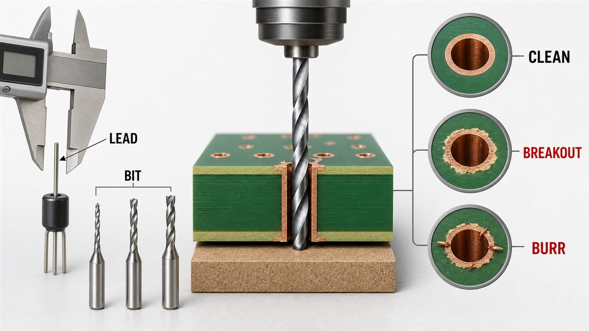
Choose the hole from the component lead, hardware diameter, plating requirement, and fit, not from a memorized universal chart. Measure the widest part that must pass through the finished hole. Then add the clearance required for assembly and tolerance. If the hole will be plated, the fabricator normally selects a larger tool diameter so the finished plated opening meets the specified final size.
| Input | What to decide | Common mistake |
|---|---|---|
| Round component lead | Measure lead diameter and specify usable assembly clearance | Matching the hole exactly to the nominal lead |
| Rectangular or formed lead | Measure the diagonal or maximum envelope | Measuring only one side |
| Connector pin group | Check pin size, pitch, and positional accumulation | Testing one pin while ignoring array alignment |
| Screw or standoff | Choose clearance, close-fit, or threaded hardware intent | Letting copper enter a mechanical NPTH keep-out |
| Plated hole | Specify finished-hole size and tolerance to the fabricator | Assuming drill-tool diameter equals finished diameter |
| Press-fit pin | Use the component supplier’s finished-hole requirement | Guessing from the pin’s nominal width |
As a starting example, a lead measured at 0.60 mm might require a finished hole larger than 0.60 mm so the part can be inserted after normal variation. The correct allowance depends on the component drawing, plating, tolerance, soldering process, and manufacturer capability; the example is not a universal specification.
How Should You Set Up the Board Before Drilling?
Place the copper board flat on clean sacrificial backing and clamp the stack so it cannot lift, chatter, or rotate. The backing supports the exit face and reduces tear-out. Confirm the drill map orientation before touching the board, especially when printed artwork was mirrored during transfer.
- Inspect the drill target under magnification and confirm that copper clearance exists around it.
- Mark or center the target accurately without cutting through nearby copper.
- Install the shortest practical length of a sharp bit to reduce runout.
- Check that the spindle is perpendicular to the board.
- Clamp the backing and PCB outside traces, pads, and the travel path.
- Make one test hole in scrap of the same material before drilling the actual board.
How to Drill a PCB Step by Step
Drill with a steady high-speed spindle and a light, straight feed; do not force the bit sideways. Carbide PCB bits cut glass-reinforced laminate cleanly but are brittle, so side load is a common cause of breakage.
- Verify the target. Match the hole location to the drill drawing, artwork, or component footprint.
- Start the spindle before contact. Let it reach stable speed without visible wobble.
- Lower vertically. Feed just fast enough to cut instead of rub; do not lever the tool.
- Break through into backing. Keep the board supported until the cutting edges fully clear the copper and laminate.
- Retract vertically. Avoid enlarging the hole by sweeping the spinning bit.
- Clear debris safely. Vacuum the work area; do not blow glass-fiber dust into the room.
- Inspect before continuing. A damaged first hole is a reason to correct setup, not repeat the same defect across the board.
Why Is Finished Hole Size Different from Drill Tool Size?
For a plated hole, the finished opening is measured after hole-wall preparation and copper plating. The factory compensates in the drilling stage so the plated finished hole meets the drawing. The compensation depends on the specified finish, process, tolerance, and fabricator capability, so designers should communicate finished-hole size rather than inventing a universal oversize value.
The annular ring must also remain after positional variation and drilling. A hole that touches or breaks through a pad edge can weaken the connection or expose an internal registration problem. Review the relationship in the PCB annular ring guide.
Can You Drill a Hole in an Existing Circuit Board?
You can physically drill some existing boards, but you should not proceed until you prove the intended location is free of top, bottom, and hidden copper, components, batteries, structural reinforcement, and hazardous stored energy. A visually blank area on a multilayer PCB may contain planes or traces.
Stop and obtain design data or engineering approval when the stackup is unknown, the board is safety-critical, the hole is close to a connector or high-current path, the board contains internal planes, or the modification could release conductive debris into an enclosure. For a mounting change, an external bracket, adhesive standoff, or enclosure revision may be safer than drilling the PCB.
What Common PCB Drilling Defects Mean
Visible symptoms usually point to setup, tool, feed, backing, or design problems. Use the defect to correct the cause before accepting more holes.
| Symptom | Likely causes | Next action |
|---|---|---|
| Off-center hole or annular breakout | Runout, poor target location, board movement, or insufficient pad margin | Stop; check fixture, bit, artwork alignment, and pad geometry |
| Raised copper burr | Dull tool, weak backing, excessive feed, or poor support | Replace the bit, improve backing, and test feed on scrap |
| Rough or fuzzy hole wall | Worn tool, rubbing, heat, or unstable spindle | Do not treat appearance alone as plating-ready; correct the process |
| Delamination or whitening | Excess force, heat, vibration, or laminate damage | Reject or escalate for engineering inspection |
| Broken bit | Side load, excess protrusion, board movement, or chipped carbide | Power down; remove fragments safely and reset the fixture |
| Component will not fit | Wrong finished-hole assumption, lead envelope error, or positional mismatch | Do not force the lead; recheck the drawing and process |
How Do You Inspect a Drilled PCB Hole?
Inspect position, diameter, edge condition, laminate condition, copper clearance, and component fit before the board proceeds. Under magnification, the pad should retain the required ring, the laminate should show no cracks or lifted fibers, and the board should remain flat. A calibrated pin gauge or appropriate measuring method is better than judging diameter by eye.
- Confirm the correct number of holes and no accidental extra holes.
- Check that each hole belongs to the correct PTH, NPTH, via, slot, or tooling class.
- Verify finished diameter and tolerance using the method required by the drawing.
- Inspect entry and exit faces for burrs, copper lifting, breakout, and delamination.
- For a modified board, perform continuity and isolation checks before applying power.
- For production plated holes, rely on the specified fabrication inspection plan rather than a visual DIY check alone.
What Drill Files and Notes Does a PCB Manufacturer Need?
A manufacturer needs unambiguous machine-readable coordinates plus human-readable fabrication requirements. Provide Gerber or ODB++ data, Excellon drill files, a fabrication drawing, board outline, stackup and thickness, PTH/NPTH definitions, finished-hole sizes and tolerances, slots/cutouts, controlled-depth requirements, and any special via treatment.
Before release, compare the drill count and sizes against the fabrication drawing and confirm that NPTH and plated holes are not merged accidentally. See how to make a Gerber file for PCB manufacturing and the broader guide to making PCB vias, plating, and DFM checks.
How Do Drill Choices Affect PCB Cost and Yield?
Drill choices affect machine time, tool changes, registration margin, plating difficulty, and inspection. Many unnecessary drill diameters increase tool changes. Very small holes, high aspect ratios, controlled-depth features, blind or buried vias, laser microvias, tight positional tolerances, and press-fit requirements can require specialized processing or more controls.
Cost reduction should begin with function, not arbitrary enlargement or removal. Standardize drill sizes only when component, current, reliability, and manufacturing requirements still pass. The drilling stage also sits inside a larger fabrication route; the overview of how PCBs are made explains where drilling, desmear, plating, imaging, and testing connect.
PCB Drilling Release Checklist
- Every hole has a defined function: PTH, NPTH, via, slot, cutout, tooling, or mounting.
- Finished-hole size and tolerance are specified where they matter.
- Component lead envelopes and connector arrays have been checked.
- Plated and non-plated holes are separated correctly in the data and drawing.
- Pad diameter and annular ring support expected positional variation.
- Drill-to-copper and drill-to-edge clearances pass the chosen fabricator’s rules.
- Board thickness and aspect-ratio implications have been reviewed.
- Slots, routed openings, countersinks, counterbores, and controlled-depth features are called out.
- Excellon drill counts match the fabrication drawing and CAM preview.
- A DIY method is used only for a board whose electrical and mechanical risks are understood.
Frequently Asked Questions About PCB Drilling
What type of drill bit is best for PCB material?
Solid-carbide PCB bits are normally preferred for glass-reinforced laminate because they hold a clean cutting edge, but they are brittle and need a rigid, low-runout setup. High-speed-steel bits may tolerate handling better but generally wear faster in abrasive glass fiber.
Can I drill a PCB with a normal hand drill?
A full-size handheld drill is difficult to control for small PCB holes because of runout, low rigidity, and poor visibility. A small high-speed spindle in a drill stand or miniature press is safer and more repeatable. Use a manufacturer for plated, multilayer, or precision holes.
Why does a PCB drill bit keep breaking?
Common causes are side load, too much bit protrusion, board movement, spindle runout, forcing the feed, or using a chipped bit. Reset the fixture and test on scrap rather than installing another bit into the same unstable setup.
Do I drill before or after etching a homemade PCB?
Both sequences exist, but alignment, artwork transfer, copper support, and the chosen DIY process determine the safer order. The essential control is that targets remain visible and correctly registered and the board is supported during drilling.
Can I make a plated through-hole by drilling and adding solder?
Drilling and filling the hole with solder is not equivalent to a controlled plated copper barrel. DIY wire-through methods may connect two sides in a prototype, but they do not reproduce a production multilayer PTH or its qualified reliability.
How do I prevent copper from lifting around a drilled hole?
Use a sharp bit, rigid perpendicular setup, firm backing, light feed, and enough pad margin. Copper that has already lifted indicates process or adhesion damage; forcing a component into the hole can make it worse.
Can a laser drill any PCB hole?
Laser drilling is valuable for small controlled-depth features such as microvias, but material absorption, copper, dielectric thickness, stackup, and process sequence matter. It is not a universal substitute for mechanical drilling.
What should I send for a PCB drilling quote?
Send Gerber or ODB++, Excellon drill data, fabrication drawing, outline, stackup, board thickness, copper weights, finished-hole sizes and tolerances, PTH/NPTH definitions, slot details, quantity, and any controlled-depth or via-treatment requirements.
Send the Drill Data for a Manufacturing Review
If the design needs plated holes, multilayer registration, controlled tolerances, unusual slots, or production repeatability, send the complete fabrication package to [email protected]. Include Gerber or ODB++, Excellon drill files, fabrication drawing, stackup, board thickness, copper weight, finished-hole requirements, quantities, and any press-fit or controlled-depth notes. PCBTry can then review the data for quoting and flag questions before fabrication rather than after holes are drilled.



0 Comments