




Can You Make a PCB in Fusion 360?
Yes. Fusion Electronics can keep a schematic, a 2D PCB layout, and a 3D board model inside one linked electronics design. A workable path is to create the schematic first, convert it into a board layout, place and route the components, run electrical and physical checks, and then export Gerber and drill data for fabrication.

The software can produce manufacturing files, but exporting files is not the same as proving that a board is manufacturable. Your component footprints, board outline, layer setup, clearances, holes, and output package still need deliberate review.
What Should You Prepare Before Starting?
Prepare the circuit requirements and manufacturing limits before drawing. This prevents a neat-looking board from reaching the end of the workflow with the wrong connector, footprint, outline, or clearance.
- A circuit sketch or reviewed schematic concept
- Component manufacturer part numbers and datasheets
- Verified symbols, footprints, and pin mappings
- Target board dimensions, mounting holes, and connector locations
- Layer count, copper weight, minimum trace/space, and minimum drill assumptions
- Power, current, impedance, thermal, and isolation requirements
- Your PCB manufacturer’s file and design-rule requirements
If the enclosure already exists, define the mechanical constraints early. Fusion is especially useful when the PCB must align with a case, panel opening, heatsink, or fixed connector.
Step 1: Create an Electronics Design
Start with an Electronics Design rather than treating the schematic and board as unrelated files. Autodesk describes the Electronics Design document as the parent that manages synchronization between the schematic, 2D PCB, and 3D PCB documents.
- Create a new project and a new Electronics Design.
- Create the schematic document inside that design.
- Use clear sheet names and keep project revisions organized.
- Confirm that the schematic and future PCB documents remain linked.
Exact button names can change between Fusion releases, so use Autodesk’s current Electronics workflow documentation when the interface differs.
Step 2: Verify Libraries and Footprints
A library component is more than a schematic symbol. It should connect the logical symbol to the correct PCB footprint, pad numbers, package outline, and, when available, a useful 3D model.
| Library element | What to verify | Failure if wrong |
|---|---|---|
| Symbol | Pin names, pin numbers, power pins | Incorrect logical connection |
| Footprint | Pad pitch, dimensions, hole sizes, pin 1 | Component cannot be assembled |
| Package outline | Body size, courtyard, connector overhang | Mechanical collision |
| 3D model | Orientation and height | Misleading enclosure check |
Do not trust a library name alone. Compare it with the exact datasheet package drawing. If you build a custom component, have another person check the pin-to-pad mapping before layout.
Step 3: Draw and Check the Schematic
The schematic defines the logical circuit. Place components, connect nets, label power rails and signals, and make the design readable before moving to the board.
- Place verified components and enter useful values or part references.
- Wire nets and use consistent net names.
- Add connectors, programming headers, test points, and protection parts.
- Check polarity, pin 1, swapped gates, and hidden power pins.
- Run the electrical rule check and resolve warnings intentionally.
If schematic reading is still the difficult part, review this circuit diagram and schematic guide. A warning may be acceptable, but it should never be ignored without understanding its cause.
Step 4: Create the 2D PCB and Board Outline
Generate the 2D PCB from the linked schematic, then define the real board boundary. The board document should contain the footprints and unrouted connections derived from the schematic.
For a simple rectangular board, set the dimensions directly in the PCB workspace. For an enclosure-driven shape, Autodesk documents a mechanical workflow in which a sketch can create a 3D PCB outline and then be pushed or linked to the 2D PCB.
- Use one closed, unambiguous board contour.
- Confirm units and finished dimensions.
- Place mounting holes from mechanical datums.
- Account for connector overhang and edge clearances.
- Keep copper and components away from routed edges where required.
Step 5: Place Components for Routing and Assembly
Place fixed mechanical parts first, functional groups second, and supporting passives near the devices they serve. Good placement shortens critical routes and makes assembly and inspection easier.
Start with connectors, mounting holes, switches, LEDs, sensors, and heatsink interfaces. Then place power conversion, processors, memory, clocks, analog sections, and their local capacitors. Rotate polarized parts consistently where the circuit allows it.
Do not optimize only for the shortest airwires. Check access for soldering, rework, test probes, programming cables, and assembly tooling. The PCB layout reading guide provides additional context for interpreting component and copper relationships.
Step 6: Set Design Rules Before Routing
Design rules translate manufacturing capability and electrical needs into layout limits. Set them before routing so the tool can flag violations while decisions are still easy to change.
| Rule group | Define from | Why it matters |
|---|---|---|
| Trace width | Current, copper weight, temperature rise, fabricator limits | Reliability and manufacturability |
| Clearance | Voltage, environment, process capability | Isolation and yield |
| Via and drill | Finished hole, plating, annular ring limits | Hole quality and connectivity |
| Layer setup | Stackup and signal needs | Routing, return paths, impedance |
| Copper-to-edge | Routing method and supplier rule | Avoid exposed or damaged copper |
Use the manufacturer’s published limits as a starting point, then request an engineering review for unusual stackups or tolerances. General software defaults are not a substitute for project-specific DFM requirements.
Step 7: Route Traces, Plan Vias and Copper
Route the power and critical signals deliberately before filling the remaining connections. Preserve a clear return path and avoid creating unnecessary detours through split copper areas.
- Route clocks, sensitive analog nets, high-current paths, and constrained pairs first.
- Keep decoupling loops short and connect them with practical trace or plane geometry.
- Change layers with vias only when it improves the routing or return path.
- Use copper pours intentionally and confirm that narrow islands or slivers are removed.
- Finish ordinary signals, then inspect the whole board at high zoom.
For hole-related manufacturing details, see the PCB drilling and hole-quality guide. A via is not just a dot on screen; its drill, pad, annular ring, plating, and layer connection must all be manufacturable.
Step 8: Run ERC and DRC
Run the electrical rule check on the schematic and the design rule check on the PCB. Resolve every error, and document why any remaining warning is acceptable.
- Unconnected or accidentally crossed nets
- Clearance and trace-width violations
- Overlapping footprints or silkscreen on pads
- Insufficient annular rings or invalid drill sizes
- Copper too close to the board edge or slots
- Unrouted connections and isolated copper
- Missing solder-mask openings or unintended openings
A zero-error DRC means the board satisfies the rules you entered. It does not prove that the rules were correct, so compare the setup with your manufacturer before approving the design.
Step 9: Review the 3D PCB
The 3D PCB view helps reveal mechanical conflicts that are difficult to see in a flat layout. Check board position, component height, connector access, mounting hardware, enclosure walls, cable bend space, and keep-out areas.
Treat placeholder 3D packages cautiously. A clean 3D rendering is not evidence that the footprint or pin numbering is correct. The datasheet and verified package definition remain the controlling references.
Step 10: Export Gerber and Drill Files
Use the CAM Processor in the 2D PCB document to create the fabrication outputs requested by your manufacturer. Autodesk lists Gerber and ODB++ among the supported manufacturing formats, along with drill, pick-and-place, BOM, netlist, and documentation outputs.
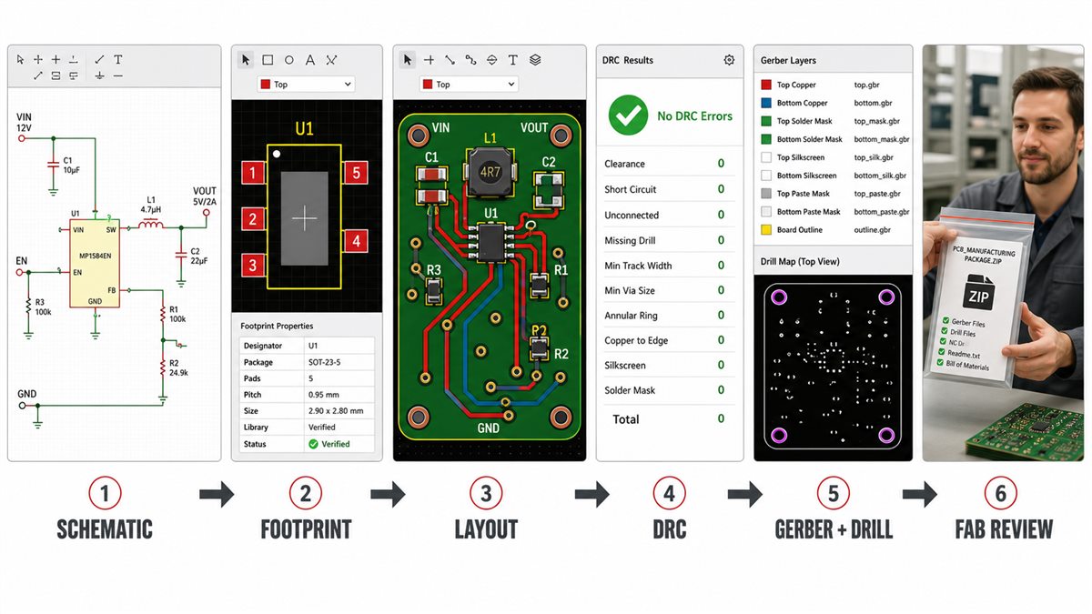
- Select a CAM job that matches the required layer set.
- Export copper, solder mask, silkscreen, profile, and drill data.
- Keep plated and non-plated hole information clear.
- Open the exported files in an independent Gerber viewer.
- Confirm outline alignment, layer polarity, apertures, text, and drill registration.
Read the PCB Gerber file guide before sending the package. Exporting a ZIP without viewing it is one of the easiest ways to pass a preventable mistake to fabrication.
What Files Should You Send to a PCB Manufacturer?
For a bare PCB quotation, send the fabrication package plus a concise specification note. Assembly requires additional component and placement data.
| File or note | Purpose | Check before sending |
|---|---|---|
| Gerber or ODB++ package | Copper, mask, silkscreen, profile | All intended layers present and aligned |
| Drill files | Plated and non-plated holes | Units, tool sizes, hole types |
| Fabrication drawing or notes | Stackup, finish, thickness, special requirements | No conflict with digital files |
| Readme | Revision and project-specific instructions | Current revision clearly identified |
| BOM and pick-and-place | Assembly quotation and placement | MPNs, polarity, rotation and coordinates reviewed |
Ask for a DFM review when the design uses fine features, unusual materials, controlled impedance, special via structures, routed slots, tight mechanical tolerances, or other nonstandard requirements. This DFM and DFA overview explains why design checks and assembly checks are related but not identical.
Fusion 360 PCB Mistakes That Cause Manufacturing Delays
The most expensive mistakes usually come from incorrect inputs or incomplete review, not from one missed toolbar command.
- Choosing a symbol with the wrong footprint or pin mapping
- Changing the schematic and board without preserving synchronization
- Drawing an open, duplicated, or incorrectly scaled board outline
- Routing with default rules that do not match the fabricator
- Using a mechanical hole where a plated electrical hole is required
- Leaving text, copper, or mask features outside the intended profile
- Sending Gerbers without an independent viewer check
- Forgetting revision notes, stackup requirements, or controlled-impedance information
A Final Fusion 360-to-Fabrication Checklist
Use this checklist before releasing the design:
- Schematic and PCB are linked and synchronized.
- Every critical symbol, footprint, pad number, and polarity mark matches the datasheet.
- Board outline, dimensions, holes, connector positions, and keep-outs match the mechanical design.
- Layer setup, trace widths, clearances, vias, drills, and copper-to-edge rules match manufacturing needs.
- ERC and DRC results are clean or every accepted warning is documented.
- 3D review covers enclosure fit, heights, access, cables, and hardware.
- Gerber/ODB++, drill, profile, mask, and silkscreen outputs have been viewed independently.
- Revision, stackup, finish, thickness, quantity, impedance, and special requirements are stated.
- Assembly jobs include a checked BOM and pick-and-place file.
When the package is ready, send the same reviewed ZIP and specification note used for your final check to the manufacturer. This makes the quotation easier to compare and gives engineering a consistent basis for DFM feedback.
Frequently Asked Questions
Is Fusion 360 suitable for PCB design?
Fusion Electronics supports schematic capture, 2D PCB layout, routing, 3D board integration, design-rule checks, and manufacturing output. It is particularly useful when electronic and mechanical design must stay connected.
Can Fusion 360 export Gerber files?
Yes. Autodesk documents manufacturing output through the CAM Processor, including Gerber and ODB++ options. Always inspect the exported layers and drill data before sending them to a manufacturer.
Should I start with the schematic or the 3D board?
Most projects should start with a linked Electronics Design and schematic. An enclosure-driven project may define the mechanical outline early, but the logical circuit and physical PCB must remain synchronized.
Can I create a PCB from a Fusion sketch?
Yes. Autodesk documents creating a PCB from a closed mechanical sketch and then pushing or linking that outline to the 2D PCB. Confirm units, contour closure, mounting datums, and the final profile layer.
Does a clean DRC mean the PCB will work?
No. DRC confirms compliance with the entered physical rules. It cannot prove circuit function, correct footprints, appropriate current capacity, return-path quality, thermal performance, or correct manufacturing assumptions.
What is the difference between ERC and DRC?
ERC checks logical electrical issues in the schematic, while DRC checks physical layout rules such as clearance, width, overlap, drill, and board-edge constraints. A production release should review both.
Do I need a separate Gerber viewer?
Yes. An independent viewer checks what was actually exported rather than what the editable design appears to contain. Review every layer, the outline, drill registration, mask openings, and text orientation.
What should I send for PCB assembly?
In addition to fabrication and drill data, assembly normally needs a BOM, pick-and-place data, polarity and orientation information, assembly drawings or notes, and any programming or test requirements.
Ready for a Manufacturing Review?
Send your reviewed Gerber or ODB++ package, drill files, board specifications, quantity, and special requirements through the pcbtry contact or quotation channel. For assembly, include the BOM and pick-and-place file. Engineering review should confirm the file package and manufacturability before production.



0 Comments