




How do you use photosensitive dry film for a PCB?
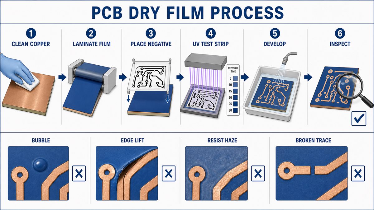
Clean and dry the copper, remove the film’s inner protective liner, laminate the resist without trapped air, place a dense negative artwork against it, calibrate UV exposure with a test strip, then remove the outer liner and develop the unexposed areas. Do not etch until every pad, clearance and thin track looks continuous under magnification.
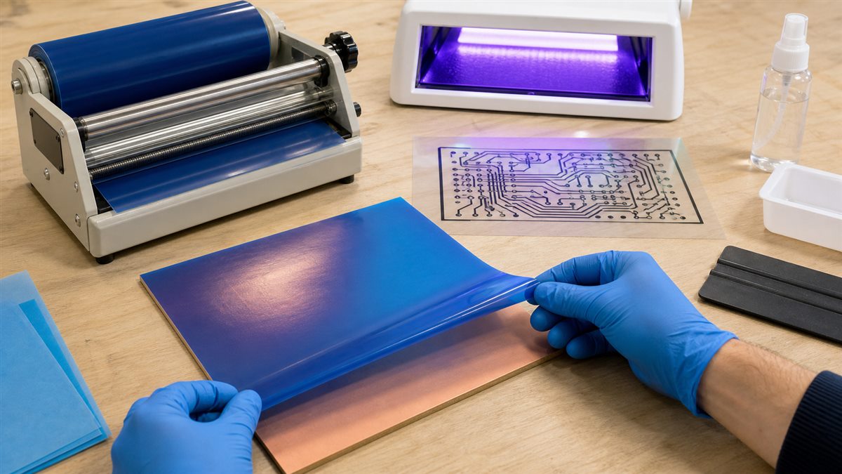
What does negative dry film photoresist do?
Negative dry film hardens where ultraviolet light reaches it. The dark areas of a negative artwork block light, so those unexposed resist areas dissolve during development and reveal copper for etching. This is the opposite of treating the blue film as a printable sticker: its two clear liners, light sensitivity and development chemistry are functional parts of the process.
Tools and materials to prepare
- Copper-clad board, dry film resist and the supplier’s data sheet
- Fine abrasive pad, detergent, lint-free wipes and clean water
- Hot-roll laminator or temperature-controlled iron with clean paper
- Dense negative artwork, clear carrier and a flat glass contact frame
- UV source, timer and an opaque card for a stepped exposure test
- Developer recommended for the film, separate trays, gloves and eye protection
- Magnifier, plastic tongs and the chosen copper etchant
Use compatible containers and follow the chemical supplier’s handling and disposal instructions. Never mix spent solutions or pour them away without checking local requirements.
Prepare the copper for reliable adhesion
Dry film sticks to clean copper, not to fingerprints, oxide or polishing residue. Cut the board with safe handling margins, smooth sharp edges, scrub evenly until water sheets across the surface, rinse and dry without touching the imaging area. Be ready to laminate immediately because freshly cleaned copper begins oxidizing again.
Laminate the dry film without bubbles
- Cut the film slightly larger than the board and identify its two transparent liners with small pieces of tape at a corner.
- Remove only the liner on the adhesive side. Keep the top liner in place during lamination.
- Tack one edge squarely, then feed the board through a warm laminator while keeping light tension on the film.
- Make another pass only if the material data sheet permits it. Excess heat or repeated passes can distort the resist.
- Let the board cool flat and trim the excess film, leaving the top liner intact until after exposure.
A small bubble over scrap copper may be harmless; a bubble crossing a track or pad is a reject because the artwork-to-copper geometry is no longer controlled.
Prepare a dense negative artwork
For common negative dry film, copper that must remain should be clear on the artwork and copper to be removed should be opaque. Confirm this against the film instructions before exposing a real board. Print at 100% scale, verify a known dimension, inspect black areas against a bright lamp and orient the printed side against the resist to minimize light spreading.
Calibrate UV exposure instead of copying a time
Exposure time changes with film batch, lamp wavelength, distance, artwork density and contact pressure. Make a stepped test: cover most of a laminated coupon with an opaque card, expose one band, move the card by the same distance, and repeat. Develop the coupon and choose the shortest exposure that holds fine tracks and pads while clearing spaces cleanly.
Develop the image to a clear endpoint
After exposure, peel off the remaining top liner and place the board in freshly prepared developer at the concentration and temperature specified for that resist. Agitate gently. Development is complete when unwanted resist has cleared to bright copper and the hardened pattern no longer changes. Overdevelopment can attack thin features; stopping early leaves a haze that prevents even etching.
Inspect the pattern before etching
Rinse, dry and inspect under strong side light and magnification. Check every narrow neck, annular ring, isolated pad and tight clearance. A continuity tester cannot validate bare photoresist; you must visually confirm the mask before copper is removed. Repair only small, unambiguous defects with a compatible resist pen. Re-laminate if defects affect repeated features or critical spacing.
Dry film troubleshooting table
| Symptom | Likely cause | Next correction |
|---|---|---|
| Film lifts at edges | Oxide, fingerprints, cold board or poor edge pressure | Re-clean, dry fully and verify lamination temperature |
| Bubbles or silver patches | Film laid down too quickly or moisture/debris trapped | Tack one edge and laminate progressively on a clean board |
| Whole image washes away | Underexposure, wrong artwork polarity or wrong liner removed | Check polarity and repeat a stepped exposure coupon |
| Spaces will not clear | Overexposure, light leakage, weak developer or artwork not opaque | Improve artwork contact/density and recalibrate |
| Thin tracks break during development | Underexposure, excessive development or features below the process window | Select a stronger test step and relax feature size |
| Good resist but etched tracks narrow | Etch undercut or excessive etch time | Improve agitation/process control and review PCB etch factor |
Etch, strip and verify the board
Etch only after the resist passes inspection. Keep the board moving as recommended for the etchant and stop when unwanted copper has cleared; extra time increases undercut. Rinse thoroughly, strip the hardened resist with the compatible remover, then inspect track widths and clearances before drilling or assembly.
When should you move from DIY film to factory fabrication?
DIY dry film is useful for learning, quick single-sided fixtures and process experiments. Use professional fabrication when the design needs plated through-holes, controlled multilayer registration, solder mask, fine repeatable features, impedance control, documented inspection or production quantities. Export and review your PCB Gerber files, drill data and fabrication notes rather than sending only a screenshot.
Pre-etch dry film checklist
- Copper is uniformly clean and has not been touched.
- Only the adhesive-side liner was removed before lamination.
- No bubble crosses a pad, track or clearance.
- Artwork polarity and 100% scale are verified.
- Printed artwork faces the resist and lies flat.
- Exposure came from a developed test strip, not a copied timer value.
- Open copper is bright and free of blue haze.
- Every critical feature passes magnified inspection.
Frequently asked questions
Which protective layer comes off first?
Remove the liner covering the adhesive resist surface before lamination. Keep the other liner on during lamination and exposure, then remove it before development. Test a scrap corner if the layers are difficult to identify.
Can I use an ordinary clothes iron?
It can work for experiments, but pressure and temperature are less uniform than a laminator. Use clean paper between iron and film, avoid sliding, and validate the result on a coupon.
How long should I expose PCB dry film?
There is no universal time. Calibrate your exact lamp, distance, artwork and film with a stepped exposure test.
Why does the film not stick?
The usual causes are oxidized or contaminated copper, residual water, insufficient heat or pressure, and touching the active surface.
Why does all the resist disappear in developer?
Check for underexposure, reversed artwork polarity, the wrong liner still present, or incompatible developer before changing several variables at once.
Why are clearances still blue?
The artwork may leak light, contact may be poor, exposure may be excessive, or the developer may be exhausted. A test coupon separates exposure trouble from development trouble.
Can dry film make very fine tracks at home?
It can resolve fine features, but the usable limit also depends on artwork density, contact, dust, exposure and etch undercut. Design to the process you have demonstrated repeatedly.
Is dry film the same as solder mask?
No. Imaging dry film used as an etch resist is removed after patterning copper. Permanent solder mask has different materials, curing requirements and service conditions.
What files should I send for professional fabrication?
Send Gerber or another accepted fabrication dataset, NC drill files, board outline, layer stack and notes for material, copper thickness, finish, quantity and special testing.
Get the design checked before fabrication
If your prototype now needs plated holes, multilayers or repeatable production, send the Gerber files, drill files, board dimensions, material, copper thickness, surface finish, quantity and test requirements through the PCBtry contact page. An engineering review can identify file gaps and manufacturability risks before quotation.



0 Comments