




How can a laser engraver make a PCB?
The most accessible method is to coat clean copper with a laser-compatible etch resist, use the laser to remove the resist where copper must be etched, inspect the pattern, then etch and strip the board. Some fiber or specialized lasers can ablate copper directly, but a result from one laser type cannot be copied safely to another.
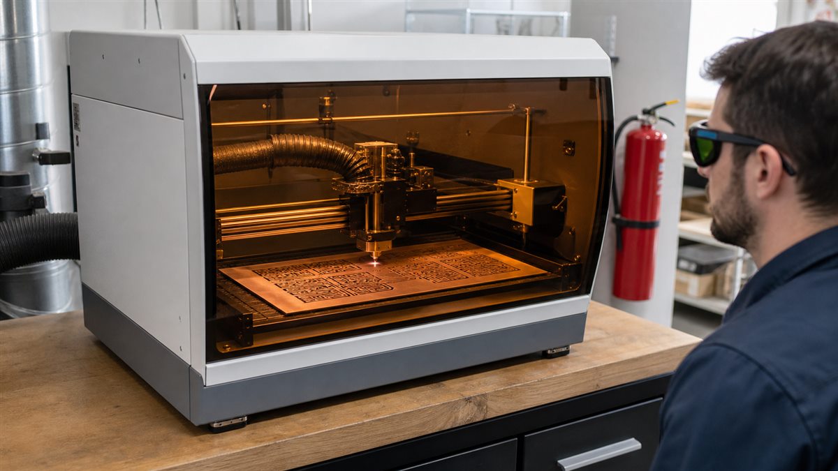
Choose the correct laser PCB route
| Route | Laser action | Next process | Best use |
|---|---|---|---|
| Mask ablation | Removes a thin approved coating | Chemical etch | Common diode/CO2 experiments |
| Direct copper ablation | Removes or isolates copper | Clean and inspect | Compatible fiber/specialized systems |
| Marking only | Changes surface appearance | Not a conductive pattern process | Labels and traceability |
Check material and laser safety first
Use the laser manufacturer’s approved material list, enclosure, interlocks, extraction and eye protection. Copper can reflect laser energy, and burned coatings create fumes. Do not laser PVC, vinyl, unknown laminates or an unidentified paint. Keep a suitable fire response nearby and never leave the machine running unattended.
Prepare a manufacturing image with correct polarity
Export the copper layer at 1:1 scale and confirm whether black means “remove mask” in your laser software. Delete page borders and unintended board outlines, preserve holes or registration marks as separate operations, and verify a known dimension. Start from reviewed Gerber data rather than a low-resolution screenshot.
Clean and coat the copper evenly
Degrease and lightly prepare the copper so water sheets across it. Apply only a coating known to be compatible with the laser and etchant. Thin spots expose copper prematurely; thick or glossy areas may need excess laser energy. Let the coating cure exactly as its instructions require.
Focus, fixture and run a calibration matrix
Clamp the coupon flat on a nonflammable fixture and set focus using the machine procedure. Engrave a grid that changes one variable at a time: power across columns and speed or passes across rows. Choose the lowest-energy cell that removes the mask cleanly without scorching the laminate or widening the intended opening.
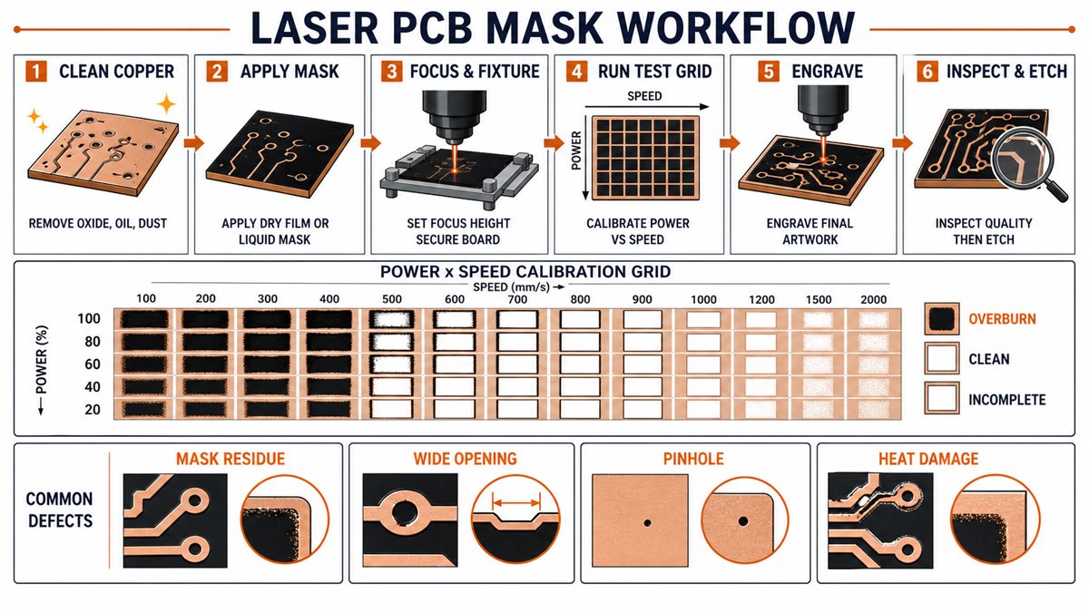
Engrave the mask and inspect before etching
- Home the machine and confirm the artwork origin.
- Run a low-power frame or boundary check if supported.
- Engrave with the selected coupon settings.
- Use magnification to check every clearance, pad and narrow track.
- Remove loose residue without scratching protected areas.
- Reject the mask if pinholes, merged gaps or registration errors affect the circuit.
Etch and strip the board
Use a compatible etchant with gloves, eye protection and local disposal rules. Stop when unwanted copper clears; extra exposure increases undercut. Rinse, strip the remaining mask with its approved remover, then inspect continuity and isolation. Review PCB etch factor when narrow traces lose width.
Diagnose laser PCB defects
| Defect | Likely cause | Correction |
|---|---|---|
| Mask remains in openings | Low energy, poor focus or thick coating | Recalibrate on a coupon |
| Opening is wider than artwork | Too much energy, defocus or multiple passes | Reduce energy and verify focus |
| Random copper pinholes | Dirty board or uneven coating | Improve cleaning and coating control |
| Tracks narrow after etch | Mask opening plus etch undercut | Shorten etch and increase design margin |
| Laminate darkens or blisters | Excess heat or incompatible process | Stop; do not use that setting/material |
Know the limits of a laser-made PCB
A home laser workflow does not automatically provide plated through-holes, controlled multilayer registration, production solder mask, impedance control or documented inspection. Feature capability is whatever your repeated coupons and finished-board measurements prove, not a number from another machine’s video.
When professional fabrication is the better next step
Use factory fabrication for multilayers, fine-pitch assembly, plated holes, controlled impedance, repeat quantities or product qualification. Submit Gerber and drill files, stackup, material, copper thickness, finish, quantity and test requirements so the quote reflects the real design.
Laser PCB checklist
- Laser and coating compatibility are documented.
- Enclosure, extraction and fire controls are active.
- Artwork polarity, scale and origin are verified.
- Copper is clean and coating is uniform.
- Power/speed came from a coupon matrix.
- No mask residue remains in etched areas.
- No pinhole crosses a trace or pad.
- Finished continuity and isolation are tested.
Frequently asked questions
Can a diode laser engrave copper directly?
Many hobby diode setups are used to remove a coating rather than cleanly ablate reflective copper. Confirm the documented capability of the exact machine.
Can a CO2 laser remove PCB copper?
CO2 systems generally interact better with organic coatings than bare copper, so mask removal is the usual route. Follow the machine maker’s material guidance.
Is black spray paint a safe etch mask?
Only use a coating whose composition, laser behavior and etchant compatibility are known. An unknown paint may produce hazardous fumes or poor adhesion.
What power and speed should I use?
There is no universal setting. Lens, focus, wavelength, coating and machine calibration change the result; build a coupon matrix.
Can I laser cut FR-4?
Do not assume it is safe. FR-4 cutting can create hazardous fumes and damaged edges, and many machines prohibit it. Use approved mechanical routing when required.
Why are my PCB traces too thin?
The laser opening may be oversized, etching may be excessive, or both. Measure the mask before etching to separate the causes.
Can this method make double-sided boards?
It can image both sides, but accurate registration and reliable via connections remain difficult without a controlled process.
Do I still need Gerber files?
Yes. Gerber or another controlled manufacturing dataset preserves scale and geometry and is also needed when the prototype moves to a factory.
When should I stop making the PCB at home?
Move to professional fabrication when the design needs plated holes, multilayers, fine pitch, repeatability, controlled impedance or formal quality records.
Send the prototype for manufacturing review
To convert a laser prototype into a production board, send Gerber and drill files, dimensions, stackup, material, copper thickness, finish, quantity and test requirements through the PCBtry contact page.



0 Comments