




How do you make a flexible PCB?
To make a flexible PCB, first define how the circuit must bend, choose a polyimide-and-copper construction, design the circuit around the bend zone, release complete fabrication data, and have a flex-capable factory image, etch, drill, plate, coverlay, profile, reinforce, and electrically test the board. The important work happens before fabrication: a flex circuit must be designed as a moving mechanical part, not merely as a thin rigid PCB.
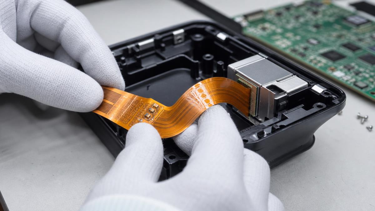
Start with the movement the flex circuit must survive
Write down where the circuit bends, the available bend radius, whether it bends only during installation or repeatedly in service, and what pulls on each end. A static flex that folds once inside an enclosure is a different design problem from a cable that cycles every time a lid opens. Also define temperature, vibration, connector mating force, assembly method, and the maximum allowed outline.
Draw the installed shape and mark fixed, transition, and active-bend regions. This simple mechanical sketch gives the PCB designer and fabricator more useful information than the word “flexible” alone.
Choose the simplest construction that meets the task
| Construction | Good fit | Main design concern |
|---|---|---|
| Single-layer flex | Simple jumpers, sensors, membrane-style circuits | Limited routing and no plated interlayer connection |
| Double-layer flex | More routing density and ground distribution | Added thickness reduces flexibility |
| Multilayer flex | Dense circuits where a connector cannot replace the flex | Stackup, via reliability, cost, and bend stiffness |
| Rigid-flex | Components on rigid islands joined by flexible sections | Rigid-to-flex transitions and fabrication complexity |
Do not add layers simply because routing is difficult. First review component placement, connector pin order, trace escape, and whether part of the circuit belongs on a rigid board.
Select flex materials as a stackup, not separate labels
A common flex construction uses polyimide dielectric, copper foil, adhesive or adhesiveless bonding, and polyimide coverlay. The correct combination depends on layer count, finished thickness, bend use, copper weight, temperature, and the fabricator’s qualified process. Rolled-annealed copper is often considered for repeated bending because its grain structure can better suit flexing, while electrodeposited copper may be acceptable for static applications. Treat that as a design discussion with the fabricator, not a universal material shortcut.
Specify finished thickness and critical material requirements in the fabrication drawing. A generic note such as “use Kapton” does not define a manufacturable stackup.
Define bend zones before routing
A bend zone is the region expected to curve in the installed or operating shape. Keep it clear of abrupt geometry changes and items that concentrate strain. The required radius depends on total thickness, copper construction, layer count, bend angle, and whether the motion is static or dynamic; ask the chosen fabricator to validate the actual stackup rather than copying one ratio from a generic chart.
- Mark the bend centerline, direction, angle, and available radius.
- Keep plated holes, component pads, and rigidener edges outside the active bend.
- Avoid changing trace width inside the bend.
- Avoid sharp inside corners in the flex outline.
- Keep the bend away from the rigid-to-flex transition.
- Tell the fabricator whether the bend is installation-only or repeated.
Route copper to reduce concentrated strain
Route traces smoothly through the bend and, where practical, perpendicular to the bend axis. Use curved or gradual direction changes instead of sharp corners. Stagger conductors on adjacent layers rather than stacking them directly when the qualified stackup and electrical requirements allow it. Avoid solid copper features that unnecessarily stiffen an active bend; a suitable hatched pattern may help in some designs, but it must still meet current, impedance, shielding, and fabrication requirements.
Neck-downs, teardrops, pad transitions, and copper-to-edge clearance should follow the fabricator’s flex rules. A desktop rigid-board rule set is not enough.
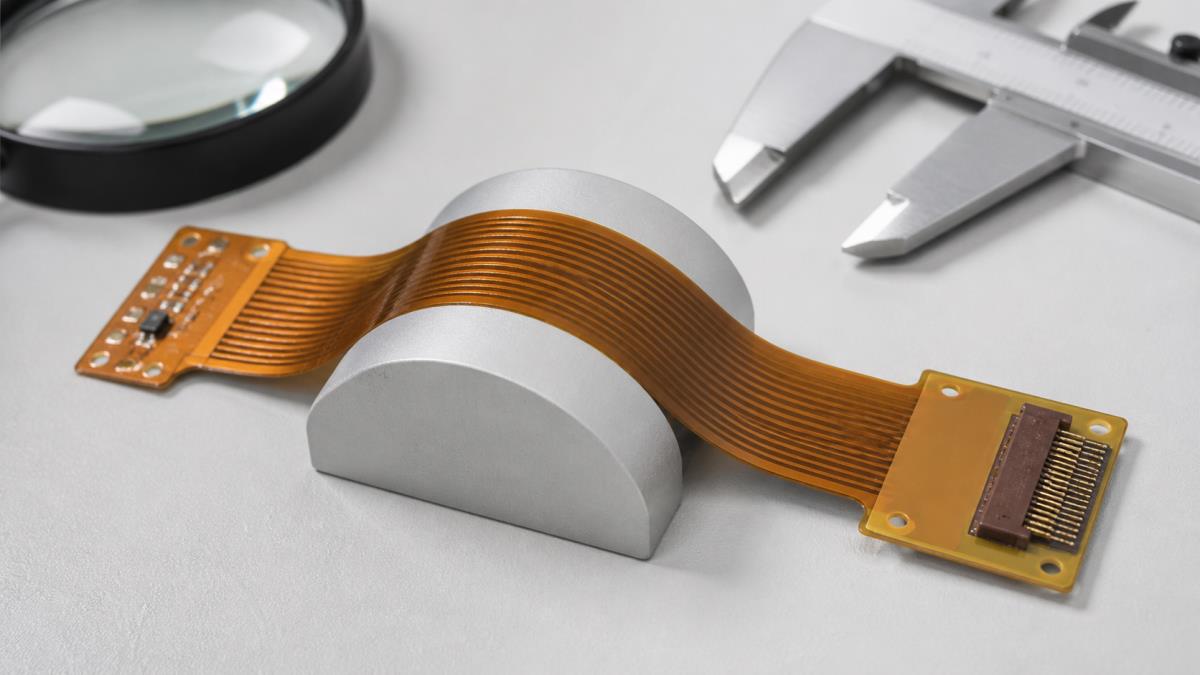
Use coverlay openings deliberately
Coverlay protects the copper but behaves differently from liquid photoimageable solder mask. Define openings for pads and exposed contacts with the manufacturer’s registration capability in mind. Closely spaced openings may merge into a larger window. Review the exposed copper, coverlay web width, annular coverage, and access needed for soldering or connectors.
If a contact area needs a surface finish, specify it clearly. Do not assume that every exposed pad needs the same finish or that a finish suitable for soldering is automatically suitable for repeated connector contact.
Add stiffeners where parts and connectors need support
A stiffener supports a region that should not bend, such as a ZIF contact tail, through-hole connector, or component area. Define its material, thickness, outline, alignment, and whether adhesive is required. Check the final thickness demanded by the mating connector. Place the stiffener edge away from the active bend or use a suitable transition so the edge does not become a strain concentration point.
Place components only on mechanically controlled regions
Unless a component and assembly process are specifically qualified for flexing, keep components outside active bend zones. Provide enough stable area for paste printing, placement, reflow, inspection, and handling. Review tall or heavy parts for peel force and vibration. If components must sit on a flexible section, define local support and confirm the assembly fixture with the supplier.
Prepare a complete flexible PCB release package
| Release item | What it must communicate |
|---|---|
| Gerber or ODB++ data and drill files | Copper, coverlay openings, outline, holes, exposed contacts, and controlled features |
| Fabrication drawing | Stackup, materials, finished thickness, copper, finish, tolerances, stiffeners, and notes |
| Bend drawing | Bend zones, direction, angle, radius, static/dynamic use, and installed shape |
| Netlist or IPC-356 data | Independent electrical-test reference |
| Assembly package | BOM, centroid/CPL, assembly drawings, polarity, panel and fixture needs |
| Acceptance requirements | Electrical, dimensional, visual, impedance, and bend-related checks required by the project |
Open the final fabrication data in an independent viewer. Confirm that coverlay, stiffener, outline, slots, copper, and drills line up; these items are easy to mis-map when a rigid PCB template is reused.
Understand the factory fabrication sequence
- Engineering review: the factory checks stackup, spacing, bend areas, tooling, panelization, and release-data consistency.
- Material preparation: qualified flexible laminates and coverlay materials are prepared with controlled handling.
- Imaging and etching: the copper pattern is transferred and unwanted copper is removed.
- Drilling and plating: holes are produced and plated when the construction requires electrical interconnection.
- Layer registration and lamination: multilayer structures are aligned and bonded using the approved process.
- Coverlay application: patterned coverlay is aligned and laminated over the circuit.
- Surface finish and stiffeners: exposed contacts receive the specified finish and support regions are added.
- Profiling and electrical test: the flexible outline is produced and continuity/isolation is verified against the net data.
- Final inspection and packing: dimensions, appearance, marking, cleanliness, and specified mechanical checks are reviewed before protected shipment.
Review DFM before ordering prototypes
Ask the intended fabricator to review the real files and proposed stackup. Confirm minimum trace and spacing, copper-to-edge distance, via and pad construction, coverlay registration, stiffener tolerances, panel support, surface finish, impedance needs, and expected bend use. If a rule is critical, put the agreed value in controlled documentation instead of leaving it in an email thread.
Inspect the finished flexible PCB before assembly
| Check | Method | Warning sign |
|---|---|---|
| Outline and stiffener position | Drawing comparison and measurement | Edge or thickness interferes with connector/enclosure |
| Coverlay registration | Magnified visual inspection | Pad coverage or inadequate web |
| Copper and transition areas | Visual inspection under suitable lighting | Crack, crease, nick, or sharp stress point |
| Continuity and isolation | Electrical-test record or approved test | Open, short, or intermittent result |
| Installed bend | Controlled fit trial using the intended radius | Buckling, whitening, excessive force, or contact movement |
| Cleanliness and packing | Visual and handling review | Residue, scratches, uncontrolled folding, or moisture exposure |
Avoid these common flex PCB mistakes
- Routing first and deciding the bend location later
- Putting vias, pads, stiffener edges, or components in the active bend
- Using a rigid-PCB stackup note for a flexible construction
- Leaving the manufacturer to guess whether bending is static or dynamic
- Ignoring connector tail thickness and stiffener tolerance
- Releasing coverlay as though it were ordinary solder mask
- Forcing a multilayer flex where a simpler flex-plus-rigid-board architecture would be more robust
- Approving production before an installed-shape prototype is checked
Flexible PCB FAQ
Can I make a flexible PCB at home?
Simple experimental circuits can be made from copper-clad flexible film, but chemical handling, feature control, plated holes, coverlay registration, multilayer alignment, and repeatability limit home methods. Use a qualified fabricator for a board that must meet controlled dimensions or reliability requirements.
What material is used for flexible PCBs?
Polyimide is a common dielectric, combined with copper foil and coverlay. Adhesives, stiffeners, finishes, and exact thicknesses depend on the stackup and application.
Is a flexible PCB the same as a rigid-flex PCB?
No. A flexible PCB is built primarily from flexible materials. A rigid-flex PCB integrates rigid board sections and flexible interconnect sections into one structure.
How many layers can a flexible PCB have?
Flex circuits may be single-layer, double-layer, or multilayer. More layers increase routing capacity but also thickness, stiffness, manufacturing complexity, and cost.
What is the minimum bend radius?
There is no single safe value for every flex circuit. It depends on thickness, copper, layer count, bend angle, construction, and cycle requirement. Get the proposed stackup and bend condition reviewed by the fabricator.
Can vias be placed in a bend area?
They should normally be kept outside active bend regions because the hole and pad create a local stiffness and stress concentration. Any exception needs explicit engineering qualification.
Why does a flex PCB need a stiffener?
A stiffener makes a local region mechanically stable for a connector, component, or assembly operation. It is support, not an extra electrical layer.
Do flexible PCBs use solder mask?
They commonly use patterned coverlay over flexible regions. Some constructions may use flexible solder-mask materials in suitable areas, but the choice and registration rules should be agreed with the manufacturer.
What files should I send for a flex PCB quote?
Send fabrication data, drill data, a fabrication and stackup drawing, bend information, material and finish requirements, quantity, and assembly files when PCBA is required.
Should I prototype the installed bend?
Yes. A flat electrical test cannot prove enclosure fit or mechanical behavior. Test the board in its intended shape and, for dynamic use, define an appropriate cycle-validation plan.
Request flex PCB DFM and quotation review
Before ordering, send the fabrication package, stackup target, bend drawing, quantity, finish, and assembly requirements through the PCBTRY contact page. Ask for a flex-specific DFM review so materials, bend zones, coverlay, stiffeners, panel support, and acceptance requirements are confirmed against the intended manufacturing process.



0 Comments