




The PCB blind via fabrication process creates a plated connection from an outer copper layer to one or more internal layers without drilling through the complete board. Blind vias free routing space, shorten unused via stubs and help escape fine-pitch packages, but they also make layer access, drilling depth, hole cleaning and copper distribution more demanding than a conventional plated through-hole.
The manufacturing route must be agreed before the stack-up is frozen. PCBtry reviews the proposed layer spans, dielectric construction, drill data, copper requirements and acceptance plan, then returns DFM questions tied to the actual build. Send Gerber or ODB++, NC drill files, stack-up, impedance requirements and fabrication notes to [email protected] for an engineering review and quotation.
What Is the PCB Blind Via Fabrication Process?
A blind via begins at a finished outer surface and stops on a specified internal copper layer. The fabrication process must expose that target layer at the correct manufacturing stage, form the hole without damaging the capture pad, remove residue, deposit continuous copper into a closed-end cavity and verify the connection after later thermal and lamination cycles.
“Blind via” describes where a via starts and ends; it does not define one universal hole size or drilling method. A laser-drilled microvia is often blind, but a larger controlled-depth mechanical hole can also be blind. The approved stack-up, via depth, diameter, material system and reliability class determine the route. For a broader comparison of structures, see blind and buried vias in PCBs.
How Does the PCB Blind Via Fabrication Process Work?
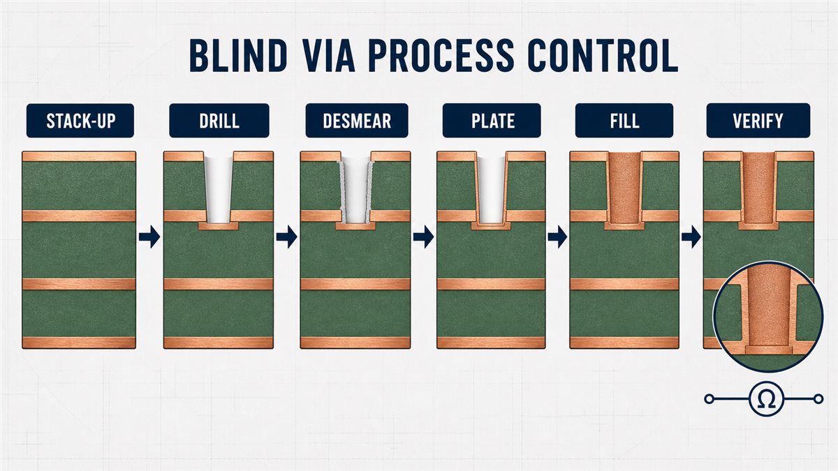
The PCB blind via fabrication process is a coordinated sequence of stack-up review, subassembly preparation, drilling, cleaning, metallization, copper build-up, lamination and verification. A defect introduced early may remain electrically invisible until reflow or thermal cycling, so each stage needs its own control and evidence.
1. Engineering review and layer-span mapping. CAM engineers compare the drill pairs with the stack-up and identify when every target layer is physically accessible. They also review finished hole intent, pad geometry, copper weights, sequential-lamination cycles and whether the via will be filled or capped. A layer span that cannot exist at the planned drill stage forces a stack-up change; discovering this after routing usually creates expensive redesign.
2. Inner-layer imaging and subassembly preparation. The target internal layers are imaged, etched and inspected before they become inaccessible. Registration targets and tooling references are created for later lamination and drilling. Incorrect inner-layer compensation or an undersized capture pad can turn normal material movement into breakout, reduced annular connection or a missed target.
3. Lamination to the required drill stage. The fabricator bonds the layers needed for that blind-via span. Sequential build-up designs may repeat lamination, drilling and plating for different via levels. Resin flow, dielectric thickness and panel movement must stay compatible with registration and the planned via depth. Voids or excessive movement can compromise both the hole and the surrounding conductor geometry.
4. Laser or controlled-depth mechanical drilling. Laser drilling removes thin dielectric to reach a capture pad and is common for small build-up vias. Controlled-depth mechanical drilling serves larger or deeper structures when the construction supports it. The control is not simply “hit the depth”: the process must maintain location, hole shape and target-pad integrity. Over-drilling can damage the pad; insufficient energy or depth leaves dielectric at the bottom; drill wander can reduce the effective land.
5. Desmear and via-bottom preparation. Drilling can leave resin residue, redeposited material or glass-rich surfaces that interfere with metallization. Chemical or plasma preparation cleans and conditions the cavity so copper can bond to the hole wall and target pad. Under-cleaning can create a weak or intermittent interface; aggressive treatment can attack the dielectric or change the hole geometry. The correct recipe is material- and construction-specific.
6. Electroless copper and electrolytic plating. A thin conductive deposit first covers the prepared cavity, after which electroplating builds the required copper. Blind-hole geometry makes solution exchange and current distribution different from an open through-hole, especially near the bottom corner. Poor wetting, trapped gas, contamination or an unsuitable depth-to-diameter relationship can produce voids or thin copper where the barrel meets the target pad.
7. Filling, planarization and further build-up when specified. Via-in-pad or stacked constructions may require the blind via to be filled and the surface made flat before another copper layer or component pad is formed. Incomplete fill can leave dimples or cavities; poor planarization can disturb imaging and assembly. If another via is stacked above it, the lower structure must provide a sound foundation and survive additional lamination heat.
8. Final circuit formation, inspection and testing. The board continues through outer-layer imaging, solder mask, surface finish, profiling and electrical test. AOI can verify accessible copper patterns, while representative microsections reveal hole geometry, target-pad contact, copper distribution and fill condition. Electrical test confirms continuity and isolation at that moment, but high-reliability projects may also require agreed coupons, thermal stress or cycling evidence because a marginal interface can pass initially and fail later.
| Process stage | Critical control | Likely failure if control is weak | Useful evidence |
|---|---|---|---|
| Layer-span review | Accessible target layer and correct drill pair | Unbuildable stack-up or wrong connection | Approved stack-up and drill-span table |
| Drilling | Registration, depth and target-pad condition | Pad damage, residue or breakout | Drill map, process review and microsection |
| Desmear | Clean, bondable via wall and bottom | Weak copper interface or intermittent open | Representative microsection and process control record |
| Plating | Continuous copper at the barrel and bottom corner | Void, thin copper or thermal-fatigue initiation | Copper measurement and cross-section |
| Fill/planarization | Complete fill and flat surface | Dimple, cavity or poor stacked-via support | Cross-section and surface inspection |
| Final verification | Continuity, isolation and agreed reliability margin | Latent open after assembly or service | Electrical test plus specified coupon/reliability results |
Which Blind Via Construction Route Should You Use?
Choose the route from the actual via span, dielectric depth, hole geometry, pad pitch and reliability requirement. Do not call out “laser blind via” merely because the layout is dense; the supplier must confirm that the material and copper opening are compatible with the selected laser process.
| Route | Typical fit | Primary process concern | DFM question |
|---|---|---|---|
| Laser-drilled build-up via | Short outer-to-adjacent-layer connection and dense routing | Target-pad cleanliness, taper and copper at the bottom corner | Which dielectric/copper construction is qualified for this via? |
| Controlled-depth mechanical blind via | Larger hole or deeper span supported by the stack-up | Depth tolerance, tool geometry and target-layer damage | How is depth referenced and verified on this panel? |
| Sequential build-up with multiple via levels | Several HDI transitions across different layer pairs | Registration accumulation, repeated lamination and cost | How many build-up cycles are required, and can spans be simplified? |
| Filled and capped via-in-pad | Fine-pitch BGA escape or a component land over the via | Fill quality, planarization and surface finish flatness | What fill/cap specification and inspection evidence apply? |
A through-hole or backdrilled via may be a lower-risk alternative when routing space permits. Compare electrical performance, board thickness, layer access and total process cycles rather than assuming a blind via is automatically better.
How Does Stack-Up Design Control Manufacturability?
The stack-up determines when the target copper layer is exposed, how deep the hole must be, how many lamination cycles are needed and how much registration movement the design must tolerate. This makes blind-via planning a stack-up decision before it is a CAD drill setting.
For example, an outer-layer-to-adjacent-layer build-up via can be drilled after that dielectric is laminated over its capture pad. A span across several layers may require a different subassembly or controlled-depth process. Two desired spans can conflict if the required layers are never exposed together during one viable process stage.
Give the fabricator a table listing every via type, start layer, stop layer, finished intent, fill/cap requirement and associated critical nets. The DFM response should show the proposed lamination sequence, not merely state that blind vias are supported. Review related HDI PCB construction choices when build-up layers or microvias drive the design.
What Are the Main Blind Via Manufacturing Challenges?
The hardest controls are accurate registration to a hidden target, clean via-bottom preparation, uniform copper inside a cavity with one opening, and survival through subsequent thermal cycles. These risks compound rather than act independently.
- Layer registration: panel movement can shift the drilled hole relative to the internal land, reducing the real copper connection even if the nominal CAD pad looks generous.
- Residue at the target pad: dielectric or smear can block metallization and create an interface that is electrically unstable.
- Gas and solution exchange: a closed-end cavity can trap bubbles or receive less fresh plating solution at the bottom.
- Copper distribution: the via mouth may build differently from the bottom corner, so surface appearance cannot prove internal copper integrity.
- Fill and planarization: voids, dimples or over-polishing can affect the next copper layer or component land.
- Repeated thermal exposure: sequential lamination and assembly reflow stress copper/dielectric interfaces and can reveal a marginal structure.
The practical response is to simplify layer spans where possible, use supplier-preferred—not merely advertised minimum—geometry, and define representative cross-sections and coupons before fabrication.
How Does Design Affect Blind Via Reliability?
Design controls the margin available to manufacturing. Via depth relative to diameter, capture-pad size, dielectric choice, stacked versus staggered placement, copper balance and the number of lamination cycles all influence reliability.
A designer should not copy a universal aspect-ratio limit from a blog and treat it as a guarantee. Capability depends on drilling method, material, copper opening, plating chemistry, panel format and acceptance class. Ask the selected fabricator for its qualified production rule for the exact construction, then design with margin around that rule.
Stacked microvias deserve special review because an upper via transfers load through the lower filled structure. Staggering can reduce direct stress concentration but consumes routing area. The choice should be tied to the product’s thermal exposure and evidence plan, not only escape-routing convenience.
What Inspection and Testing Evidence Should Buyers Request?
Request evidence that answers four different questions: Was the hole placed correctly? Is the internal copper connection sound? Does the finished net pass? Is the structure suitable for the intended thermal environment? No single test answers all four.
| Inspection or test | What it can show | Limitation |
|---|---|---|
| AOI | Accessible conductor pattern defects and registration indicators | Cannot see the complete internal via interface |
| X-ray, when suitable | Gross fill or alignment anomalies in some constructions | Resolution and overlapping copper can limit interpretation |
| Microsection | Hole shape, target-pad contact, copper distribution and fill condition | Destructive sample represents selected locations |
| Electrical test | Finished-net continuity and isolation | A marginal interface may still pass initially |
| Thermal-stress or cycling coupon | Resistance stability through agreed thermal exposure | Meaning depends on coupon design and acceptance criteria |
Specify the applicable drawing revision, sampling plan and acceptance standard. “100% electrical test” is valuable, but it should not replace internal-structure evidence for a blind-via design with elevated reliability risk. For general bare-board verification context, see this PCB testing guide.
What Drives Blind Via Cost and Lead Time?
Blind-via cost and schedule are driven by added engineering, dedicated drill programs, sequential lamination cycles, material availability, fill/cap operations, tighter registration controls and extra qualification evidence. The smallest advertised feature is not the only cost driver.
A single via can trigger a special process route for the entire panel. Likewise, several via spans may require separate drill and plating cycles even if each individual hole looks simple. Prototype timing also changes when stack-up approval, material procurement, microsection review or reliability coupons are required.
Ask the quote to identify the proposed construction, number of lamination/drill cycles, fill/cap scope and test plan. This makes redesign decisions easier than comparing one total price with no process explanation.
How Do You Choose a Blind Via PCB Manufacturer?
Choose a manufacturer that can explain how your layer spans will be built and how internal copper quality will be proven. A capability table is only the beginning.
- Send the complete stack-up and drill-span table before routing is locked.
- Ask whether each geometry is a qualified production rule or only a special review case.
- Confirm the drilling method, lamination sequence and fill/cap route in writing.
- Ask how the supplier controls target-pad registration and via-bottom preparation.
- Agree on microsection locations, coupon design, sampling and acceptance criteria.
- Confirm change control for laminate, copper foil, chemistry or process-route substitutions.
- Request a DFM response that marks risks and alternatives, not only “can make.”
For broader supplier evaluation, PCBtry’s HDI PCB manufacturing capability page provides a useful starting point for an engineering discussion.
PCB Blind Via Fabrication Process FAQ
Is every blind via a microvia?
No. Blind describes the layer connection; microvia describes a small via structure defined by the applicable design/manufacturing context. Many laser microvias are blind, but larger controlled-depth blind vias also exist.
Are blind vias always laser drilled?
No. Laser drilling is common for shallow, small build-up vias, while controlled-depth mechanical drilling can suit larger or deeper structures. The stack-up and fabricator’s qualified process decide the method.
What causes a blind via open circuit?
Possible causes include missed target-pad registration, residue at the via bottom, incomplete seed coverage, plating voids, thin copper or cracking after thermal stress. Cross-section and resistance-based failure analysis should locate the mechanism.
Can a blind via connect more than two layers?
It can span from an outer layer to a deeper internal layer if the construction and process sequence make that target accessible. Deeper spans may change drilling, plating and lamination risk, so they require supplier review.
Should stacked or staggered microvias be used?
Staggered vias often reduce direct structural dependency but use more routing area. Stacked vias can save space but require qualified filling, registration and reliability controls. Select from density and thermal requirements together.
Can electrical testing prove blind via reliability?
Electrical test proves continuity and isolation at test time. It does not by itself show copper distribution or predict survival through assembly and service, so critical builds may need microsections and agreed thermal evidence.
What files are needed for a blind via PCB quote?
Send Gerber or ODB++, NC drill files separated by layer pair, stack-up, fabrication drawing, finished copper, impedance requirements, fill/cap notes, quantities and acceptance/test requirements.
How early should the fabricator review blind vias?
Before the stack-up and escape routing are frozen. Early review can change layer spans, via placement or construction while those changes are still inexpensive.
Send the Right Files for a Blind Via DFM Review
Prepare Gerber or ODB++, NC drill files with clear start/stop layers, the proposed stack-up, fabrication drawing, finished copper, impedance table, material constraints, via fill/cap requirements, quantities and acceptance notes. Highlight critical BGA escapes and high-reliability nets. Email the package to [email protected] and request a blind-via manufacturability review, evidence plan and quotation before design release.



1 Comment
PCB Drilling Process: Tool Control, Hole Quality and Inspection Checks - thindry pcb manufacturer · 08/29/2026 at 11:46
[…] plated from non-plated data, avoid ambiguous slots, and review HDI structures early. PCBtry’s blind-via fabrication process and via manufacturing guide provide related design […]