




The PCB SMT assembly process mounts surface-mount components onto printed solder-paste deposits and forms their electrical joints in a controlled reflow cycle. It supports dense, repeatable assembly, but the line is only as stable as its data, materials and feedback controls. A placement machine can put the wrong package in the wrong orientation very accurately if the BOM, CPL or setup is wrong.
For engineering review and quotation, send Gerber or ODB++, BOM with approved manufacturer part numbers, CPL/centroid data, assembly drawings, stencil notes, programming files and a test specification. PCBTRY can review package-to-footprint alignment, polarity, paste access, panel handling and inspection coverage before the first article is released.
What Is the PCB SMT Assembly Process?
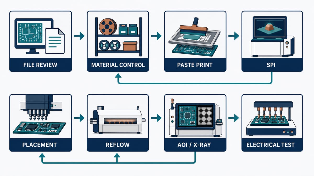
SMT assembly converts a bare PCB and component set into a populated PCBA. Components are supplied in reels, trays or tubes, placed directly on surface pads, and soldered by heating a printed paste deposit through its approved thermal process. The basic flow is file review, material preparation, stencil printing, SPI, placement, reflow, AOI or X-ray, and electrical test.
Not every product needs every inspection method. Visible chip and leaded joints can be evaluated optically, while bottom-terminated packages may require X-ray. Electrical test confirms behavior that a camera cannot see. The product design, reliability requirement and customer acceptance plan should determine the route.
How Does the PCB SMT Assembly Process Work?
The stages below form one closed process. When a defect is detected, the factory should trace it to the controlling input instead of repeatedly repairing the output.
1. Engineering file and DFM review. Engineers reconcile the PCB revision, BOM, CPL, assembly drawing and polarity information. Footprint, package, pin-one and feeder data must agree. A conflict stopped here is a clarification; the same conflict found after reflow becomes rework or scrap.
2. Material verification and traceability. The line confirms component identity, package, lot, moisture status and approved substitutions. Bare boards, paste, stencil and programs are tied to the released build revision. Uncontrolled floor life or a mixed reel can create intermittent defects that are difficult to diagnose later.
3. Stencil setup and solder-paste printing. The printer aligns the stencil to the panel and transfers paste through each aperture. Aperture design, board support, squeegee condition, separation and cleaning affect deposit shape. Too much paste can bridge; too little or an offset deposit can create opens or weak wetting.
4. Solder paste inspection (SPI). SPI checks deposit location, area, height and volume against the approved program. Its real value is feedback: a repeating offset points to alignment, while a gradual trend can indicate stencil contamination or print-condition drift. Passing an average while one critical pad repeatedly fails is not meaningful control.
5. Component placement. Pick-and-place equipment verifies feeders, recognizes parts with vision, aligns to fiducials and places each package at the programmed X/Y position and rotation. Nozzle selection, pickup quality, board support and component presentation matter. Wrong feeder loading, unclear polarity or poor fiducials can defeat nominal machine accuracy.
6. First-article verification. Before the lot runs, the first populated panel is compared with the BOM, drawing and known polarity references. This check should focus on high-risk packages, variants and substitutions rather than becoming a visual formality. A signed first article establishes that the intended configuration reached the line.
7. Reflow soldering. The assembly passes through controlled heating, soak, liquidus and cooling behavior defined for its solder paste, components and board thermal mass. Thermocouples on representative locations verify the product profile. A generic oven recipe may overheat a small component while a shielded or high-copper area still wets poorly.
8. AOI and X-ray inspection. AOI checks component presence, polarity, position and visible joint geometry. X-ray supports inspection of BGA, QFN and other hidden interfaces. Both methods require a validated program and defect disposition; false calls waste time, while loose thresholds allow escapes.
9. Rework, cleaning and secondary operations. Confirmed defects are repaired under a controlled instruction with recorded reason and result. Cleaning depends on flux chemistry and product requirements. Through-hole insertion, selective soldering, coating or depaneling follow when the assembly design requires them.
10. Electrical test and release. ICT, flying probe, programming and functional testing are selected from the product risk and available access. Test verifies nets, components or behavior that visual inspection cannot prove. Release records should connect the tested unit or lot to its assembly revision and material history.
What Files Prevent SMT Assembly Errors?
| File or input | What it controls | Frequent risk |
|---|---|---|
| Gerber/ODB++ | Pad, mask and paste geometry | Paste layer or revision differs from PCB |
| BOM | Manufacturer part, package and substitution | Generic value without orderable MPN |
| CPL/centroid | X/Y, rotation, side and reference | CAD rotation convention mismatch |
| Assembly drawing | Polarity, variants and mechanical intent | Drawing conflicts with BOM or CPL |
| Programming/test package | Firmware and acceptance behavior | No version or pass criteria |
| Approved deviation list | Substitution and rework authorization | Production change not traceable |
Version the package as one release. Our PCB prototyping process guide explains how first-build evidence should drive the next revision rather than disappear in email.
How Does Solder Paste Printing Control SMT Yield?
Printing creates the solder volume and position available to form every joint. The key judgment is not whether paste is visibly present, but whether deposits are repeatable and suitable for the pad/package combination. Board support and cleanliness matter because a panel that lifts from the stencil can smear deposits even when machine settings appear unchanged.
| SPI pattern | Likely process question | Correct response |
|---|---|---|
| All deposits shifted similarly | Alignment, fiducial or board position | Stop and correct registration |
| One aperture gradually loses volume | Stencil blockage or underside contamination | Clean and verify the next print |
| Random tall/irregular deposits | Paste roll, separation or board support | Check print mechanics and material condition |
| Repeated bridge-prone fine-pitch pattern | Aperture/land relationship | Review stencil design with DFM |
How Are Placement and Polarity Verified?
Placement verification begins before the nozzle moves. The feeder setup must match the approved BOM; the machine package library must match the physical part; and polarity references must agree among data, drawing, part marking and footprint. Barcode or independent setup verification reduces reliance on memory.
AOI can detect many wrong, missing or rotated parts after reflow, but it should not be the first time polarity is considered. First-article review is especially important for LEDs, diodes, electrolytic capacitors, IC pin one, connector variants and substitute packages.
How Is the Reflow Profile Approved?
A profile is approved from measurements on a representative populated assembly, not solely from the oven’s displayed zone temperatures. Thermocouples should represent both heat-sensitive and high-thermal-mass locations. The measured curve is compared with the solder paste and component requirements, then linked to the product recipe.
Our SMT reflow oven guide provides equipment context, but an oven capability does not replace a board-level profile record.
What Defects Point to Which SMT Process Stage?
- Bridges: review paste volume/alignment, land design, placement and reflow behavior.
- Opens: check missing paste, wetting, coplanarity, placement and pad condition.
- Tombstoning: compare deposit symmetry, placement, pad geometry and thermal balance.
- Wrong or reversed part: audit BOM, feeder setup, polarity rules and first-article approval.
- Hidden-joint voiding or non-wet: review paste, component/PCB finish and reflow with X-ray evidence.
- Intermittent functional failure: correlate electrical results with material lot, rework and process history.
What Inspection and Test Evidence Should Buyers Request?
Ask for evidence proportional to the build risk: file-review disposition, first-article approval, SPI/AOI program status, profile record, selected X-ray images, electrical test result and rework history. A machine list says what the factory owns; these records show how the process was controlled for your product.
For hidden-joint products, connect X-ray criteria to the package and acceptance requirement. For prototypes, preserve actual defect and rework data rather than reporting only final pass quantity. For production, request traceability that can isolate affected lots without quarantining unrelated builds.
How Do You Choose an SMT Assembly Supplier?
- Can engineering reconcile BOM, CPL, drawings and polarity before setup?
- How are substitutions, feeder loading and material lots authorized and traced?
- Does SPI feed corrections back to printing, and are trends reviewed?
- How is a representative reflow profile measured and released?
- Which joints receive AOI, X-ray and electrical test, and why?
- How are rework reasons recorded and verified?
Clarify whether your scope is SMT-only or a mixed assembly that also needs through-hole assembly, programming, coating or functional test.
Frequently Asked Questions
What is the basic SMT assembly sequence?
File review, material control, paste printing, SPI, placement, first article, reflow, AOI/X-ray and electrical test form the core sequence.
Why is SPI placed before component placement?
It detects paste problems while the board can still be cleaned and reprinted. It also provides feedback to stabilize the printing process.
Does AOI replace electrical testing?
No. AOI evaluates visible assembly features; it cannot prove firmware, power sequencing, interfaces or every electrical connection.
When is X-ray needed?
It is commonly considered for hidden joints such as BGA and bottom-terminated packages, or when a specific defect investigation requires internal evidence.
What causes an SMT component to be reversed?
Typical causes are inconsistent polarity data, wrong feeder orientation, library errors or an ineffective first-article check.
Can one reflow recipe be used for every PCB?
No. Board mass, copper, package mix and material limits change thermal behavior. Approve a measured product-specific profile.
What files are needed for an SMT quotation?
Provide Gerber/ODB++, BOM, CPL, drawings, quantity, substitutions, programming and test requirements.
How should rework be controlled?
Use an approved instruction, qualified tools and a recorded defect/disposition, then reinspect and retest the repaired assembly.
Request an SMT Assembly Engineering Review
Send PCBTRY your Gerber or ODB++, BOM, CPL, assembly drawings, quantity, substitution rules, programming and test package. We can review data alignment, package risk, paste/inspection coverage and the evidence needed for a controlled quotation and build.



0 Comments