




High-frequency PCB lamination bonds patterned RF cores, bonding films or prepregs, copper foils and supporting layers into one multilayer structure without losing the dielectric thickness, registration and material properties assumed by the RF design. Unlike a routine FR-4 build, the press cycle cannot be chosen from the word “Rogers” or “PTFE” alone. Each laminate and bonding family has its own storage, surface preparation, flow, temperature and pressure requirements.
The practical goal is a board whose final stackup still matches the field-solver model and survives drilling, plating, assembly and service. PCBTRY supports material and stackup review, DFM, fabrication and inspection. Send Gerber/ODB++ data, the controlled stackup, material callouts, impedance table, finished thickness, copper requirements and RF acceptance notes for an engineering review and quotation.
What Is the High Frequency PCB Lamination Process?
The high frequency PCB lamination process is the controlled heat-and-pressure bonding of RF circuit layers into a multilayer PCB. The adhesive may be a thermoset prepreg, a low-loss bondply, a thermoplastic film or a material-specific bonding system. Its electrical properties become part of the transmission-line geometry, so it is not merely structural glue.
Complexity increases when a stack combines PTFE or hydrocarbon-ceramic RF cores with FR-4 support layers. Different expansion, resin flow, copper roughness and dimensional movement can change registration, flatness and dielectric spacing. The fabrication drawing therefore needs an exact material family and construction, not a generic “high-frequency material” note.
How Does the High Frequency PCB Lamination Process Work?
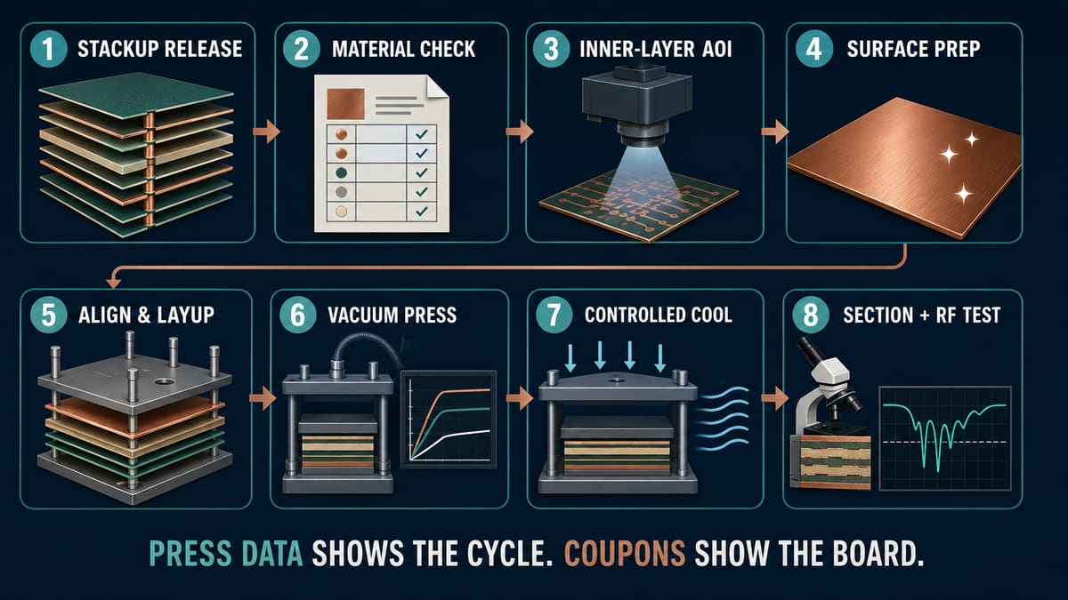
1. Engineering review and DFM analysis. The fabricator checks material availability, copper type, dielectric targets, impedance structures, via sequence, panel size and final thickness. This prevents a stackup that is electrically modeled but cannot be pressed or registered. Unresolved substitutions can shift impedance or loss, so the buyer should receive an approved production stackup before material is cut.
2. Stackup and bonding-system definition. RF cores, bondply/prepreg, copper foils and support layers are assigned by exact family and thickness. The bonding layer must meet both electrical and processing needs. A convenient FR-4 prepreg can add unwanted loss to an otherwise low-loss construction; an incompatible film can also create adhesion or sequential-lamination limits.
3. Material receiving, storage and conditioning. Lot identity, shelf/storage requirements, copper surface and material condition are verified. Moisture or volatile contamination can create blisters or voids. Conditioning must follow the material supplier’s fabrication guide because an indiscriminate bake can harm a bond-enhancing surface or alter handling.
4. Inner-layer imaging, etching and inspection. Circuit layers are patterned, then inspected for line geometry, copper defects and registration targets. RF lines and couplers may be sensitive to etch variation. Lamination cannot restore lost conductor geometry, so inner-layer AOI and coupon data should be accepted before layup.
5. Surface preparation and layup. Copper and dielectric surfaces are cleaned or treated using a process compatible with the chosen materials, then stacked with tooling and separator systems. Over-aggressive treatment can change copper profile or damage a specialty dielectric; insufficient preparation can reduce adhesion. The work traveler should identify the approved preparation route.
6. Registration and dimensional compensation. Layers are aligned with tooling or optical systems using compensation derived from material behavior and panel history. Specialty cores can move differently from FR-4 during etch and press. Poor compensation produces annular-ring loss, layer-to-layer RF discontinuity and coupon-to-board mismatch.
7. Vacuum pressing, heating, pressure and cooling. The stack follows a recipe qualified for the selected bonding system. Vacuum helps remove trapped air, while heat, pressure and dwell produce flow, wetting and cure or fusion. Excess flow can starve local areas and change dielectric thickness; insufficient flow can leave voids. Controlled cooling limits stress and warpage.
8. Post-lamination verification and release. The panel is checked for thickness, flatness, registration, voids, bond integrity and material movement before drilling. Microsections and coupons verify the actual construction; impedance or RF tests verify the electrical result when specified. A press chart alone proves that a recipe ran, not that the product met the stackup.
What Materials Are Used in High Frequency PCB Lamination?
The material set includes the RF core, copper foil and a compatible bonding layer. Hybrid boards may also include FR-4 cores or prepregs for routing, power distribution or mechanical support. Selection should start from loss budget, dielectric tolerance, thermal exposure, layer count and fabrication route.
| Material element | Engineering question | Lamination risk to control |
| PTFE-based RF core | Is reinforcement, copper type and surface treatment defined? | Dimensional movement, adhesion and drilling preparation |
| Hydrocarbon-ceramic RF core | Which matching bondply/prepreg is approved? | Mixed-flow behavior and final dielectric thickness |
| Low-loss prepreg or bondply | Do Dk, Df, flow and cure fit the model and process? | Added loss, voids or resin starvation |
| Thermoplastic bonding film | Can the construction and later thermal cycles support it? | Reflow or sequential-lamination limitations |
| FR-4 support material | Does its loss and expansion affect the RF structure? | CTE mismatch, warpage and unplanned loss |
| Copper foil | Is copper profile included in the RF model? | Conductor loss and adhesion tradeoff |
How Is the RF Stackup Released for Lamination?
Release the RF stackup with actual material names, target dielectric thicknesses, copper weights/profiles, finished thickness, impedance structures and allowed substitutions. A nominal layer count is not enough. The fabricator should return the proposed production stackup so the designer can rerun the field solver when values change.
- Mark which layers carry controlled RF structures and which are supporting digital/power layers.
- Identify core construction versus foil construction where it affects surface dielectric and vias.
- Define sequential lamination only when the via architecture requires it.
- Show reference planes, copper balancing and any cavity or mixed-thickness features.
- State coupon, impedance, S-parameter or other acceptance needs before quotation.
What Are the Key Lamination Challenges?
The dominant challenges are material compatibility, dielectric-thickness control, layer registration, trapped volatiles and hybrid-stack stress. They interact: changing bonding material to improve flow can change loss or thickness, while increasing copper treatment to improve adhesion can increase conductor loss.
| Failure signal | Likely control gap | Evidence to request |
| Local delamination or blister | Contamination, conditioning, surface preparation or cure | Material lot record, traveler, press chart and microsection |
| Impedance shift after fabrication | Final dielectric or trace geometry differs from model | Actual stackup, coupon geometry and test trace |
| Layer-to-hole registration loss | Material movement or compensation error | Registration coupon and X-ray/section data |
| Panel bow or twist | Asymmetric copper/materials or cooling stress | Stackup symmetry review and flatness measurement |
| Voids near dense copper | Air removal or resin-flow path inadequate | Cross-section/ultrasonic evidence as applicable |
How Does Design Affect Lamination Reliability?
Design controls the copper distribution, resin-flow paths, thermal balance and registration margin available to manufacturing. Large copper-free areas beside dense features can produce uneven flow; an asymmetric hybrid stack can warp; tight pad-to-hole geometry leaves little allowance for material movement.
Reliability improves when the designer and fabricator close the loop before release. Let the fabricator propose manufacturable dielectric values, then update the RF model and freeze the approved stackup. Do not treat a material substitution as purchasing-only: it can change Dk, Df, cure behavior, copper adhesion and the press cycle.
What Tests Confirm Lamination Quality and RF Performance?
No single test proves lamination quality. Use a layered evidence set: incoming material identity, press-process records, dimensional inspection, registration evidence, microsections and the electrical tests specified by the design.
| Check | What it demonstrates | What it does not prove alone |
| Press chart/traveler | The qualified recipe was executed | Actual void-free bond or RF performance |
| Finished thickness mapping | Panel and local build thickness | Internal interface integrity |
| Microsection | Layer spacing, interfaces, registration and plated-hole structure | Whole-panel RF behavior |
| Impedance coupon | Transmission-line result for represented structures | Every RF feature on the board |
| S-parameter or application-specific RF test | Specified insertion/return-loss behavior | Long-term mechanical reliability unless paired with qualification |
How Long Does High Frequency PCB Lamination Take?
Lamination time is only one part of lead time. Prototype timing depends on material availability, stackup approval, tooling, press qualification, sequential cycles and required coupons or RF testing. Hybrid stacks and uncommon bondplys may add procurement and engineering time before production begins.
For a useful quotation, ask the supplier to separate material lead time, engineering approval, fabrication and test time. Do not publish or accept a generic “fast” promise without confirming the exact material, thickness, panel and test requirement.
How Should You Choose a High Frequency PCB Manufacturer?
Choose a manufacturer that can explain how the exact material family changes storage, preparation, compensation, pressing and inspection. A logo list is weaker evidence than a reviewed stackup, controlled material traceability, relevant coupons and a clear nonconformance path.
- Can the supplier obtain the specified laminate and bonding material without silent substitution?
- Will engineering return an actual production stackup for RF review?
- How is dimensional compensation established for this material and panel?
- Which surface preparation and press recipe family is used, and how is it controlled?
- What coupon, microsection, impedance and RF evidence can accompany the order?
- How are changes to material lot, foil profile or bonding layer communicated?
Frequently Asked Questions
Is high-frequency PCB lamination the same as FR-4 lamination?
The equipment may be similar, but the material handling, surface preparation, compensation and press recipe can differ. The bonding system’s supplier guidance controls the process.
Can FR-4 prepreg bond Rogers or other RF cores?
Some constructions use it, but electrical loss and process compatibility must be evaluated. The combination should be approved in the production stackup rather than assumed.
Why does bonding material affect RF performance?
It becomes part of the dielectric structure around fields and transmission lines. Its thickness, Dk and Df can change impedance and loss.
Does vacuum lamination eliminate all voids?
No. Vacuum helps remove air, but surface condition, volatile content, layup, resin flow and the press cycle still determine the bond.
What causes delamination after reflow?
Possible causes include moisture, contamination, inadequate adhesion, incomplete cure or a bonding material that cannot tolerate later thermal exposure. Cross-section and process records are needed to identify the cause.
Should I specify an exact press temperature and pressure?
Usually specify the material system and product requirements, then audit the fabricator’s qualified recipe. Copying a recipe without the exact press, stack and material history is risky.
What files are needed for quotation?
Provide Gerber or ODB++ data, stackup, drill files, impedance table, material callouts, copper requirements, panel constraints, finished thickness and test requirements.
How can I verify the final RF stackup?
Review the as-built stackup, microsection dimensions and relevant coupon results. Use impedance or S-parameter testing when the design requires direct electrical evidence.
Request a Lamination and Stackup Review
Send PCBTRY your Gerber/ODB++ package, controlled stackup, material and copper callouts, drill data, impedance structures, finished thickness and RF test notes. Engineering review can identify incompatible bonding choices, unrealistic thickness targets, registration risks and missing acceptance evidence before material release and quotation.



0 Comments