




A reliable PCB design process converts product requirements into a verified electrical design, physical layout and controlled manufacturing package. The work does not end when every unrouted connection disappears. A board is ready only when the schematic, libraries, stackup, constraints, placement, routing, mechanical data, BOM and fabrication outputs agree—and another reviewer can understand what was released.
PCBtry can review fabrication data before production. Send Gerber files, drill data, stackup, fabrication drawing, BOM, placement data and the expected build quantity through the contact page for DFM feedback and a quotation.

What Is the Goal of a PCB Design Process?
The goal is a board that meets measurable electrical, mechanical, thermal, manufacturing, assembly and test requirements. “The circuit works” is necessary but incomplete. The board must fit its enclosure, use orderable parts, survive its environment, be inspectable and produce unambiguous files.
Define success before drawing. Record supply ranges, interfaces, loads, signal timing, environment, dimensions, connectors, service life, compliance constraints, test access, prototype quantity and expected production route. Each important requirement should lead to a schematic choice, layout constraint or verification item.
What Inputs Should Be Ready Before Schematic Capture?
Start with a requirements document, block diagram, interface list, power budget, mechanical envelope and preliminary component strategy. Identify unknowns explicitly. If connector pinout, enclosure location or power source can still change, mark the dependent design area instead of pretending it is fixed.
| Input | Design decision | Evidence before release |
| Power and load | regulation, protection, copper and thermal path | budget, calculations and measured prototype plan |
| Interfaces | transceiver, termination, impedance and connector | datasheet references and constraint set |
| Mechanical model | outline, holes, keep-outs and height limits | ECAD/MCAD review |
| Manufacturing route | stackup, feature limits, panel and assembly process | supplier capability/DFM confirmation |
| Test strategy | test points, programming and fixtures | bring-up and production-test plan |
How Does the PCB Design Process Work?
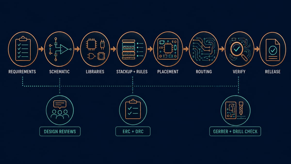
The process is iterative, but eight controlled stages make reviews and handoffs visible.
1. Define requirements and architecture. Partition power, processing, analog, communication, protection and external connections. Record constraints and failure consequences before choosing details.
2. Capture and review the schematic. Draw readable functional blocks, name important nets, show power flow, add decoupling/protection from verified references and resolve ERC messages individually. A clean ERC does not prove the circuit concept.
3. Verify symbols, footprints and parts. Compare pin numbers, package, polarity, thermal pads, pitch, height and mating direction to the exact datasheet. Link every BOM item to an orderable part and approved alternative policy.
4. Define stackup and design rules. Choose layers, reference planes, dielectric construction and copper distribution with the fabricator. Convert current, voltage, impedance, assembly and mechanical needs into net classes and rule constraints.
5. Place components. Fix outline, mounting and connectors first. Place power loops, clocks, decoupling, sensitive analog and high-speed interfaces by functional flow, return path, heat and assembly access before filling remaining space.
6. Route and review copper. Route critical networks deliberately. Inspect return continuity, layer transitions, neck-downs, plane splits, current paths, clearances, copper-to-edge distance and thermal spreading. Autorouting cannot supply system intent.
7. Verify the complete board. Run ERC and DRC, then perform manual electrical, mechanical, thermal, DFM/DFA and testability reviews. Use independent reviewers at schematic, placement and final-release milestones.
8. Generate and inspect release data. Export Gerber or accepted image data, NC drill, netlist, fabrication and assembly drawings, BOM, CPL and relevant models. Open the actual outputs in an independent viewer and archive one revision-controlled package.
How Should a PCB Schematic Be Reviewed?
Review a schematic for intent, not only connectivity. Trace each power rail from entry through protection and regulation to every load. Check reset, boot, programming, clocks, unused pins, pull states, connector direction and off-board fault exposure. Ask a reviewer to explain the circuit without relying on the designer’s memory.
Record assumptions beside the requirement or in controlled notes. A net called “5V” is not evidence that its source, current capacity and sequencing are correct.
How Are Footprints and Libraries Verified?
Library verification is a separate engineering gate because a correct schematic symbol can still map to the wrong physical package. Compare the exact manufacturer drawing to pad numbers, pitch, body size, exposed pad, courtyard, polarity and 3D/mechanical orientation.
Print critical footprints at 1:1 or compare them against controlled mechanical data. Connectors, switches, displays and polarized devices deserve independent review because a mirrored orientation can survive ERC and DRC.
How Is the Stackup Turned Into Design Rules?
The stackup establishes reference planes, dielectric thicknesses and available copper layers; design rules translate that structure into allowed geometry. Confirm the stackup before controlled-impedance routing and set rules by net function rather than one universal width/clearance.
Use the selected fabricator’s reviewed capability instead of copying “standard” values from an unrelated board. The DFM and DFA review should resolve exceptions before release.
Why Does Placement Come Before Detailed Routing?
Placement determines loop area, return paths, thermal coupling, connector stress and assembly access. A weak placement cannot be rescued by cosmetic routing. Place related components to show current and signal flow, keep decoupling connections short, protect sensitive nodes and reserve probe access.
Review placement with mechanical and assembly context visible. Height restrictions, tool access, polarity visibility, rework clearance and enclosure features change whether a mathematically connected design can be built and serviced.
What Routing Checks Matter Beyond DRC?
DRC checks encoded rules; it cannot know every functional intention. Manually trace return paths, especially across layer changes and plane boundaries. Review power voltage drop and heat, differential/controlled structures, crystal and switching loops, edge exposure and coupling between noisy and sensitive networks.
A passing DRC is the start of review evidence, not the release decision. Document any intentional rule waiver with owner, reason and affected nets.
What PCB Design Failures Cause Manufacturing Delays?
| Failure | Why it escapes | Consequence | Prevention |
| Wrong footprint | symbol connectivity passes | part cannot mount or orientation is wrong | datasheet/library review |
| Stackup mismatch | layout uses assumed construction | impedance or manufacturability query | fabricator-approved stackup |
| Missing drill/outline | CAD database looks complete | CAM hold or wrong mechanics | independent output viewer |
| Ambiguous revision | files exported separately | mixed fabrication/assembly package | single controlled release archive |
| No test access | prototype debug was manual | slow bring-up and weak production coverage | test strategy before placement |
How Should PCB Design Reviews Be Scheduled?
Review at architecture/schematic, placement and final release. The schematic review catches circuit and interface errors. Placement review catches physical, return-path, thermal and assembly problems before routing makes change expensive. Final review checks the actual outputs and revision package.
Use a reviewer who was not the sole author of the section. Track findings to closure rather than relying on a meeting conclusion.
What Files Belong in the Manufacturing Release?
A typical package includes fabrication images, NC drill, stackup, board outline and fabrication drawing. Assembly scope adds BOM, centroid/CPL, assembly drawing, polarity notes, approved substitutions, programming and test requirements. Include README/revision information when filenames alone are ambiguous.
- Use one revision identifier across every file.
- Remove obsolete outputs from the release folder.
- Verify layer polarity and drill pairing in an independent viewer.
- Confirm board dimensions and critical holes.
- State material, copper, finish, impedance and special acceptance requirements.
- Archive the exact package sent to the supplier.
How Do You Verify Gerber and Drill Outputs?
Open the generated files as a manufacturer will receive them. Check every copper, mask, legend and mechanical layer; overlay drill data; verify plated/non-plated definitions, outline, slots, polarity markings and apertures. Compare a netlist when the workflow supports it.
This check catches export configuration errors that the native CAD view cannot reveal. Do it after the final export, not on an earlier preview.
How Does Prototype Feedback Improve the Design?
A prototype should test assumptions, not merely power on. Use a controlled bring-up plan: visual/continuity inspection, current-limited power, rail checks, clocks/reset, interfaces, loads, thermal observation and functional tests. Record expected versus measured results.
Feed every discovered issue into requirements, schematic, libraries, constraints or the release checklist. A hand-added wire may prove a fix, but the controlled design and outputs must be updated before volume production.
PCB Design Release Checklist
- Step 1: Confirm requirements, interfaces and mechanical revision.
- Step 2: Close schematic/ERC findings and verify power states.
- Step 3: Verify every critical symbol, footprint and BOM part.
- Step 4: Confirm stackup and design rules with manufacturing.
- Step 5: Review placement, return paths, heat and test access.
- Step 6: Close DRC and document justified waivers.
- Step 7: Export and independently inspect Gerber/drill/BOM/CPL.
- Step 8: Freeze one signed revision package and change route.
Frequently Asked Questions
What comes first in PCB design?
Start with measurable product requirements and a functional architecture, not component placement. Power, interfaces, mechanics, environment and test strategy determine the circuit and physical constraints.
Does a clean DRC mean the PCB is correct?
No. DRC proves only the encoded geometric rules. It cannot confirm circuit intent, footprint correctness, return-path quality, thermal behavior, mechanical fit or whether exported manufacturing files are complete.
When should a fabricator review the design?
Engage the fabricator before the stackup and critical geometry are locked, then again on the final release package. Early review prevents the layout from depending on an unavailable construction or special process.
What is the difference between Gerber and CPL files?
Gerber files describe fabricated image layers. A CPL or centroid file gives component placement coordinates and rotation for assembly. Assembly also needs a BOM and clear orientation information.
Why inspect exported Gerbers separately?
The CAD database may be correct while output settings omit, invert or misclassify a layer or drill file. An independent viewer shows the package the manufacturer actually receives.
How many PCB prototypes are needed?
Quantity depends on risk, destructive tests, parallel debugging and schedule. Define what each unit must prove before ordering; do not claim that one universal prototype quantity fits every project.
Should PCB design include test points?
Yes where bring-up, production test or service requires measurement. Define access before placement so probes and fixtures can reach important rails, interfaces and programming signals.
What should be sent for a PCB design review?
Send schematic, layout or Gerber/drill data, stackup, fabrication drawing, BOM, CPL, mechanical constraints and known risk areas. State quantity, assembly scope and test expectations.
Request a PCB Design and DFM Review
Send PCBtry your schematic, Gerber files, drill data, stackup, fabrication drawing, BOM, CPL and expected quantity through the contact page. The review can identify release conflicts, manufacturability limits and missing assembly/test information before production.



0 Comments