




The outer layer PCB process creates the conductive pattern that remains visible on the two outside faces of a multilayer board. Unlike inner layers, the outer layers must form traces and plated through-hole walls in the same plating sequence, survive final etching, and still leave enough copper geometry for solder mask, surface finish, and assembly.
A useful manufacturing review therefore goes beyond asking whether a factory can “make the line width.” It checks how the image is registered, where copper is added, what protects the circuit during etching, and what evidence releases the panel. Send your Gerber data, stack-up, finished copper requirement, controlled-impedance notes, and acceptance criteria for a DFM review and quotation.
What Is the Outer Layer PCB Process?
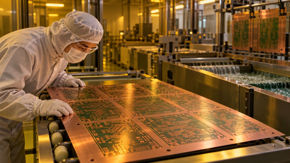
The outer layer process is the sequence that transfers the top and bottom circuit images onto a laminated, drilled panel, plates copper into the exposed pattern and holes, protects that pattern with a temporary etch resist, and removes unwanted base copper. It is more coupled than inner-layer imaging because plated holes, pads, annular rings, conductor width, and final surface geometry all depend on the same registration and electroplating decisions.
One distinction prevents a common specification error: base copper, plated copper, and finished conductor copper are not interchangeable terms. Base foil starts on the laminate. Pattern plating adds copper to exposed traces, pads, and hole walls. The finished conductor is the result after etching and cleaning. State which value your drawing controls instead of giving an unlabeled “copper thickness.”
How Does the Outer Layer PCB Process Work?
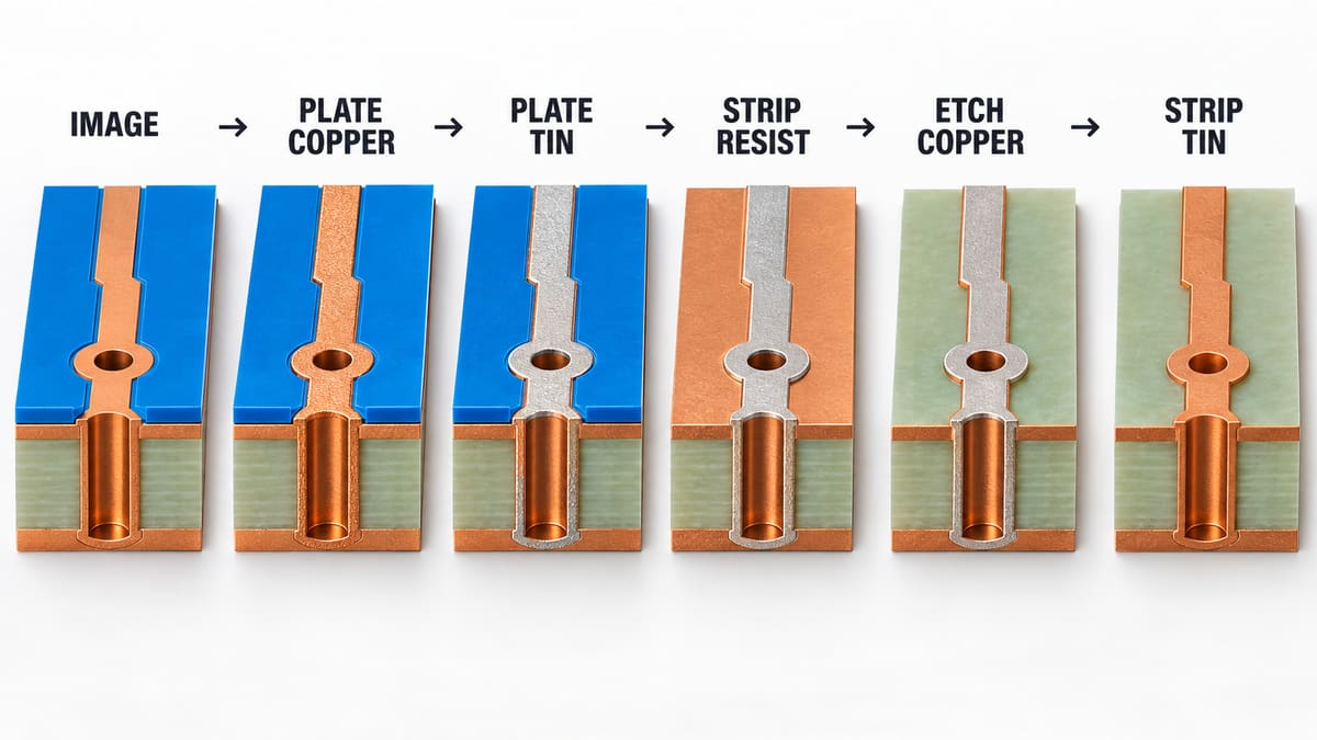
In a typical subtractive pattern-plating route, the resist opening defines where copper and then tin are deposited. After the resist is removed, tin protects the required circuit while the exposed base foil is etched away. The following steps show what each operation does, what engineers monitor, and what a loss of control produces.
1. CAM Review Sets the Manufacturable Image
CAM checks compare Gerber layers, drill data, net information, stack-up, panel orientation, copper clearances, annular rings, and impedance features. The factory may apply controlled artwork compensation for its verified imaging and etching behavior; this is not permission to alter electrical intent. An ambiguous copper callout or mismatched drill revision can produce a perfectly processed panel that is still the wrong product, so revision reconciliation is the first release gate.
2. Panel Preparation and Dry-Film Lamination Create a Clean Imaging Surface
The drilled and copper-clad panel is cleaned, micro-roughened as appropriate, dried, and laminated with photosensitive dry film. The goal is continuous adhesion without particles, trapped moisture, wrinkles, or edge lift. Poor preparation lets developer or plating solution creep beneath the resist, leading to nodules, ragged conductor edges, or unintended copper bridges.
3. Imaging and Development Open Only the Circuit Pattern
Laser direct imaging or phototool exposure aligns the top and bottom images to drilled targets. Development removes the intended resist areas so that pads, traces, and holes are exposed for plating. Registration targets and developed-feature inspection matter more than the machine name: an offset image reduces annular ring on one side, while underdevelopment leaves residue that blocks plating and overdevelopment weakens fine resist dams.
4. Copper Pattern Plating Builds Traces and Hole Walls Together
Electrolytic copper is deposited on the exposed outer-layer pattern and inside conductive holes. Current distribution, electrical contact, solution condition, agitation, panel loading, and feature density influence deposit uniformity. Thin hole copper threatens interconnect reliability; excessive or uneven surface buildup changes the conductor geometry the etching process must later preserve. Dense and open regions should therefore be reviewed as a plating-distribution problem, not only a Gerber spacing problem.
5. Tin Plating Creates a Temporary Etch Resist
A tin layer is plated over the newly deposited copper before the dry film is stripped. Its job is to protect wanted copper from the subsequent etchant; it is not the customer-selected final finish such as ENIG or HASL. Skips, pores, or poor coverage can expose wanted copper and cause local attack during etching.
6. Resist Stripping Exposes the Unwanted Base Copper
The original dry-film resist is removed, revealing the thin base foil between tin-covered circuit features. Incomplete stripping shields unwanted copper and can leave shorts or copper islands. Overaggressive chemistry or inadequate rinsing can contaminate later operations, so the panel should be visually clean before etching.
7. Etching Removes Background Copper and Defines the Final Edge
The etcher dissolves exposed base copper while tin protects the required pattern. Spray balance, chemistry condition, conveyor behavior, copper loading, and panel orientation influence lateral attack and removal rate. Because etching removes copper sideways as well as downward, the imaged width is not automatically the finished width. Fine lines beside large copper areas are especially sensitive to local loading and the PCB etch factor.
8. Tin Stripping Reveals the Copper Circuit
After etching, the temporary tin mask is stripped without damaging the underlying copper. The panel is then cleaned and inspected for residue, discoloration, edge attack, or incomplete removal. Residual tin can interfere with later surface preparation, while excessive stripping can alter exposed copper surfaces.
9. AOI and Dimensional Checks Decide Whether the Pattern Is Released
Automated optical inspection compares the manufactured pattern with CAM reference data and flags opens, shorts, neck-down, pinholes, protrusions, and spacing violations. AOI is a detection tool, not proof that every flagged feature is defective or every process is centered. Engineers review the image, confirm critical dimensions or coupons where required, and feed recurring signatures back to imaging, plating, or etching controls.
10. The Panel Moves to Solder Mask, Finish, and Electrical Test
Accepted outer circuitry proceeds to surface preparation and solder mask, legend, final surface finish, routing, and electrical test. The outer-layer operation is not complete merely because the copper looks correct: contamination or rough edges can reduce solder-mask adhesion, and an undetected conductor defect can appear only during netlist-based test. On a multilayer PCB, the released outer pattern also has to match the already laminated internal structure.
How Is Outer-Layer Processing Different from Inner-Layer Processing?
Inner layers are usually imaged and etched before lamination; outer layers are processed after lamination and drilling, so their circuit image must register to existing holes and their plating route must also build conductive hole walls. That coupling changes both the defect risk and the inspection evidence.
| Decision point | Inner layer | Outer layer | Why the difference matters |
|---|---|---|---|
| Timing | Before multilayer lamination | After lamination and drilling | Outer registration must reference the drilled, laminated panel |
| Copper formation | Foil is imaged and etched | Pattern copper is added before final etch | Finished geometry depends on both plating and etching |
| Hole relationship | Artwork must later align through lamination/drilling | Pads are imaged around existing holes | Image offset directly reduces available annular ring |
| Typical release evidence | AOI plus layer dimensions | AOI, critical dimensions, plating evidence, and later electrical test | One data source cannot prove the complete interconnect |
Which Controls Matter Most During Outer-Layer Fabrication?
The most useful controls are the ones that connect a measurable process signal to a finished-board risk. Asking only for a machine list does not show whether the process stays centered.
| Control point | What engineers verify | Loss-of-control signature | Useful buyer evidence |
|---|---|---|---|
| Data and revision | Gerber, drill, netlist, stack-up agree | Wrong pad, missing feature, layer mismatch | DFM questions and released job revision |
| Developed image | Registration, clean openings, resist integrity | Reduced annular ring, blocked plating, resist lift | Target/readback and first-panel inspection record |
| Pattern plating | Distribution across panel and hole structures | Thin hole deposit, excess surface copper, nodules | Coupon or cross-section plan tied to acceptance needs |
| Tin coverage | Continuous protection on wanted pattern | Local copper attack during etch | Process inspection and defect disposition record |
| Etching | Removal, conductor width, edge profile | Short, open, neck-down, undercut | Critical-dimension or coupon results |
| AOI release | Reference comparison and reviewed alarms | Escaped conductor defect or repeated false calls | AOI criteria and repair/disposition traceability |
What Outer-Layer Defects Point to Which Process?
A defect name is only a starting point. Its position and repeated pattern help separate data, imaging, plating, and etching causes.
- Annular ring loss in one direction: first compare image-to-drill registration and panel movement; do not assume the drill diameter alone is wrong.
- Random isolated opens: inspect for resist residue, particle-related imaging defects, tin skips, and local over-etch.
- Repeated shorts at similar dense features: examine resist dams, artwork compensation, complete resist stripping, and etch loading.
- Trace neck-down along long edges: check lateral etch, spray behavior, and the relation between starting copper, plated thickness, and feature spacing.
- Copper nodules or rough edges: review surface cleanliness, resist adhesion, plating condition, and any copper growth beneath lifted resist.
The corrective action should follow evidence. Repairing an AOI call may save one panel, but a repeating coordinate or feature class should trigger a process investigation before the next lot.
How Does PCB Design Affect Outer-Layer Yield and Reliability?
Design determines the process window before the panel reaches imaging. Small annular rings leave less registration margin; isolated fine traces beside copper pours make plating and etching balance harder; copper close to the routed edge has less mechanical and fabrication allowance; and unclear finished-copper notes invite mismatched assumptions.
During DFM, review minimum line and space by copper construction, pad-to-hole relationship, copper balance, teardrops where appropriate, impedance coupons, edge clearances, and whether exposed copper is intended for soldering, contact, or mechanical use. Do not copy a generic capability-table minimum into every feature. A repeated minimum across an entire panel is a production-yield decision, not just a CAD-rule choice.
What Tests Confirm Outer-Layer Quality?
No single inspection confirms everything. Use layered evidence that matches the failure being controlled.
- AOI: checks the imaged conductor pattern for opens, shorts, protrusions, and spacing anomalies.
- Dimensional measurement: confirms critical line, space, pad, registration, or coupon features when the drawing requires them.
- Microsection or coupon evaluation: assesses plated-hole and copper build features under the applicable acceptance plan.
- Electrical test: compares continuity and isolation to the supplied or generated netlist after fabrication.
- Visual and cleanliness checks: find residue, surface damage, contamination, or conditions that could harm solder-mask adhesion and finishing.
Specify the governing drawing and acceptance class when the application requires more than the supplier’s standard commercial release. “AOI included” and “electrically tested” are useful, but they do not define sampling, criteria, or retained records.
How Long Does the Outer Layer PCB Process Take?
Outer-layer processing is only one segment of the full board lead time. Imaging, plating, etching, AOI, and queue time are followed by solder mask, finish, profile, electrical test, and final inspection. A reliable quotation therefore gives the total build schedule after DFM rather than an isolated hours-per-operation claim.
Fine geometry, unusual copper construction, sequential qualification, special coupons, tight registration, panel rework, or an engineering hold can extend the route. Provide controlled files and resolved notes at RFQ stage; revision changes after CAM release usually cost more time than the physical exposure step.
How Should You Evaluate an Outer-Layer PCB Manufacturer?
Ask how the factory connects CAM compensation, imaging registration, pattern-plating distribution, etch control, AOI review, and electrical test. The strongest answer identifies who owns each release decision and what record can be tied to your lot.
- Send representative production data, not only a simple capability coupon.
- Ask whether your copper note means starting, added, or finished copper.
- Request the planned inspection method for critical annular rings and conductor geometry.
- Confirm how AOI alarms, permitted repairs, and nonconforming panels are controlled.
- Define the electrical-test source, acceptance standard, certificate, and retained evidence required by your program.
Outer Layer PCB RFQ Checklist
Submit the information below together so that CAM can evaluate one controlled manufacturing intent:
- Gerber or ODB++ data and NC drill/rout files with matching revision identifiers
- Readme or fabrication drawing defining stack-up, finished thickness, material and copper terminology
- Controlled-impedance values, referenced layers, trace geometry and coupon requirement
- Surface finish, solder-mask, legend, edge and exposed-copper requirements
- Applicable acceptance standard/class and any critical-dimension or microsection requirement
- Electrical-test data or permission to generate a netlist, plus certificate/record expectations
- Prototype and production quantity, panel constraints, target delivery and packaging needs
Frequently Asked Questions
Is tin plating the final PCB surface finish?
Usually not in this route. Tin temporarily protects the wanted copper during outer-layer etching and is then stripped before solder mask and the specified final finish.
Why plate copper before etching the outer layer?
Pattern plating builds the exposed traces, pads, and conductive hole walls. The plated tin then protects that required pattern while the unwanted base foil is etched away.
Does AOI replace electrical testing?
No. AOI evaluates visible pattern geometry, while electrical test checks continuity and isolation against a netlist. They control different escape paths.
What causes outer-layer over-etch?
Contributing factors can include chemistry condition, dwell time, spray balance, copper loading, feature density, orientation, and an unsuitable compensation assumption. The defect pattern and process data should be reviewed together.
Why can annular ring be lost even when the drill diameter is correct?
The outer image can be offset relative to the drilled hole, or the available pad allowance may be too small for the combined registration process. Directional loss is a useful diagnostic clue.
What copper thickness should an RFQ specify?
Label starting foil, plated copper, finished conductor copper, and hole-wall requirements separately where they matter. An unlabeled single value can be interpreted differently by designer and fabricator.
Can very fine lines be mixed with heavy outer copper?
The combination narrows the process window because added copper and longer etching influence sidewall geometry. Ask for a feature-specific DFM assessment instead of assuming two separate capability claims can be combined.
What files are needed for an outer-layer DFM review?
Provide fabrication data, drill/rout files, stack-up, copper definitions, impedance notes, finish and mask requirements, and the applicable acceptance criteria. Include one revision identifier across the package.
Get an Outer-Layer DFM Review
If conductor width, annular ring, copper build, impedance, or inspection evidence is critical to your board, send the complete fabrication package through the PCBtry contact page. We can review the outer-layer construction, identify open questions before CAM release, and prepare a manufacturing quotation based on your actual files rather than a generic capability line.



0 Comments