Blog
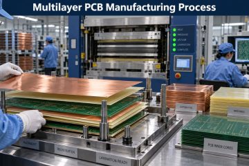
Multilayer PCB Manufacturing Process: Registration, Lamination and Testing
See how multilayer PCBs are fabricated from stack-up and inner layers through lamination, drilling, plating, inspection and electrical testing.



See how multilayer PCBs are fabricated from stack-up and inner layers through lamination, drilling, plating, inspection and electrical testing.

Learn how configurable PCB automation controls recipes, equipment data, inspection, exceptions, traceability and staged factory deployment.
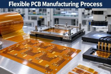
See how flexible PCBs are made from DFM and polyimide preparation through imaging, plating, coverlay, stiffeners, profiling and reliability testing.
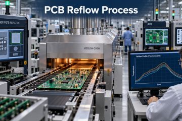
Understand the complete PCB reflow process from solder paste and placement through measured thermal profiling, oven zones, defect analysis, inspection and release.
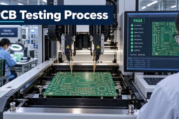
Understand the PCB testing process from in-process inspection and bare-board electrical testing to reliability qualification, release evidence and supplier checks.
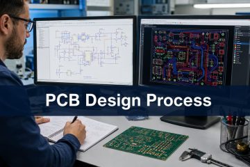
Follow a practical PCB design process from requirements and schematic capture through stackup, placement, routing, verification, Gerber review and production release.

Follow the industrial PCB manufacturing process from DFM and material control through imaging, lamination, plating, finishing, inspection, testing and supplier release.
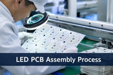
Follow the LED PCB assembly process from polarity and bin review through paste printing, placement, reflow, inspection, thermal checks, and functional testing.
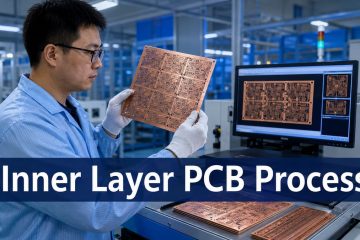
See how PCB inner layers move from CAM compensation and copper preparation through imaging, etching, AOI, oxide treatment, and lamination release checks.
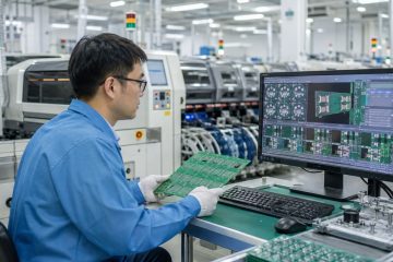
Improve PCB assembly by measuring first-pass yield, separating design and process causes, controlling print and reflow, and closing the defect-feedback loop.
If you have any enquiry about quotation or cooperation, please feel free to email us at [email protected] or use the following enquiry form. Oursales representative will contact you within 24 hours. Thank you for your interest in our products.