
Blog
PCB Blind Via Fabrication Process: Drilling, Plating and DFM Checks
See how PCB blind vias are planned, drilled, desmeared, plated and tested—and what stack-up, DFM and supplier evidence to verify before production.



See how PCB blind vias are planned, drilled, desmeared, plated and tested—and what stack-up, DFM and supplier evidence to verify before production.

See how the mSAP PCB process builds fine copper features, where plating and flash etching fail, and what DFM files and inspection evidence to request.
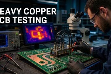
Learn how heavy copper PCBs are checked for copper geometry, plated-hole integrity, resistance, current capacity, temperature rise and reliability.

See how HDI PCBs are built through laser microvias and sequential lamination, what can fail, and which test evidence to request before ordering.

See how rigid-flex PCBs are built, which process controls prevent transition and plating failures, and what test evidence to request before ordering.
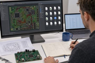
Learn how to identify and open PCB files safely, choose the right CAD or Gerber viewer, and verify layers, drills, units and revisions before manufacture.
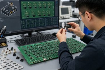
Design a hot-swappable keyboard PCB with compatible sockets, verified footprints, insertion support, matrix controls and full-key assembly testing.

Learn how PCB vias are designed, drilled, desmeared and copper plated, how via treatments differ, and which DFM files and inspection checks prove quality.
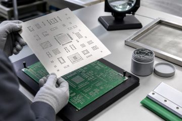
Make or order a PCB solder-paste stencil from the correct paste layers, review apertures and thickness, align it accurately, and approve the first print.
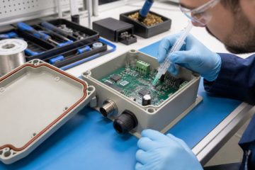
Waterproof a PCB by matching conformal coating, potting and enclosure sealing to the real exposure, then verify coverage, heat flow and product-level water tests.
If you have any enquiry about quotation or cooperation, please feel free to email us at [email protected] or use the following enquiry form. Oursales representative will contact you within 24 hours. Thank you for your interest in our products.