




How do you make PCB vias?
In professional PCB fabrication, vias are defined in the CAD stackup and drill data, drilled at the correct production stage, desmeared and metallized, then copper-plated to create a continuous barrel between selected layers. The finished via is inspected and electrically tested. On a homemade two-layer board, a wire soldered on both sides can act as a prototype layer connection, but it is not equivalent to a plated-through via.

Understand the parts of a via
A via includes the drilled hole, copper barrel, pads on connected layers and clearance or anti-pad on layers that must not connect. Solder mask may cover, expose or plug the opening. Each feature must match the stackup and fabrication capability.
Select through, blind, buried or microvia structures
| Via type | Layers connected | Primary use | Main manufacturing impact |
|---|---|---|---|
| Through via | Outer layer to outer layer | General multilayer routing | Consumes routing space through the stack |
| Blind via | Outer layer to selected inner layer | Higher routing density | Requires controlled depth or sequential build |
| Buried via | Inner layers only | Preserve outer-layer space | Must be made before final lamination |
| Microvia | Usually adjacent build-up layers | HDI and fine-pitch escape | Laser drilling and stack reliability rules |
Define the layer span in the PCB CAD tool
Assign each via to the intended start and stop layers and use the correct stackup. Do not represent a blind or buried via as an ordinary through drill with a note. The exported manufacturing data must preserve layer span and via type unambiguously.
Set hole, pad and anti-pad from capability data
Finished hole size, drill size, pad diameter and clearance are related but not identical. Drilling and plating tolerances affect the annular ring and finished opening. Use the selected fabricator’s current capability rather than copying a generic minimum.
Check aspect ratio and plating difficulty
Deep narrow holes are harder to clean and plate uniformly. Board thickness, drill diameter and via process determine the risk. When a proposed via exceeds standard capability, enlarge the hole, reduce thickness, change layer structure or use an approved advanced process.
Prepare complete drill and stackup data
Provide separate plated and non-plated drill information, tool sizes, slots and layer-span data, plus the controlled stackup. Include via-fill, cap, mask and impedance requirements on the fabrication drawing. Confirm units, zero suppression and file alignment in a CAM viewer.
Drill vias at the correct fabrication stage
Through holes are normally drilled after multilayer lamination, while buried and many blind structures require drilling and plating during intermediate build stages. Microvias are created within the sequential build-up flow. The chosen structure therefore changes the entire fabrication route.
Remove resin smear and condition the hole wall
Mechanical or laser drilling can leave resin and debris that prevent a reliable connection to inner-layer copper. Fabrication uses a controlled cleaning and desmear process suitable for the laminate. Visual cleanliness alone does not prove the inner-layer interface is sound.
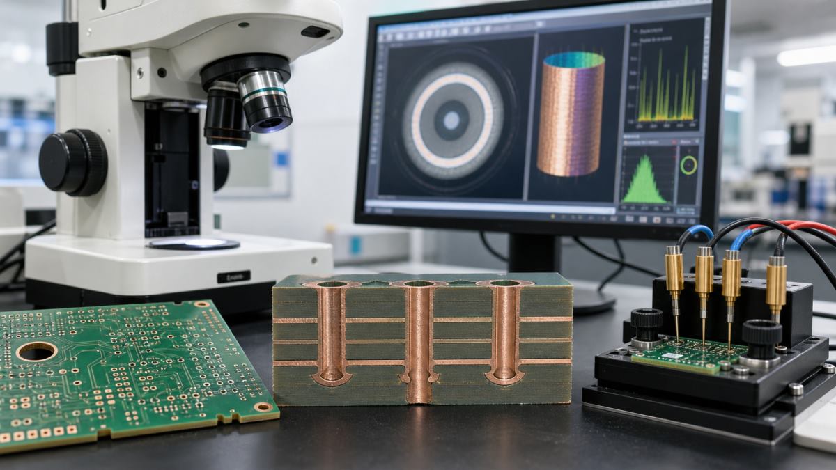
Create the conductive seed layer and plate copper
A thin conductive layer is established on the conditioned hole wall, followed by electrolytic copper build-up with the board surfaces. Process controls must produce continuous coverage through the hole. Filling a drilled hole with solder is not the normal method for creating the structural copper barrel.
Choose tented, plugged, filled or capped vias correctly
Via treatment depends on soldering, cleanliness, vacuum, thermal and via-in-pad needs. Tenting uses solder mask over the opening; plugging and filling use specified materials and processes; conductive or nonconductive fill are not interchangeable. Via-in-pad may require fill and planar copper cap before component finishing.
Keep via-in-pad requirements explicit
Open vias in component pads can wick solder and create insufficient joints or voids. If via-in-pad is required, identify the fill, planarization and cap expectation and confirm it with the assembler and fabricator. Do not assume solder mask alone will create a flat sealed pad.
Inspect vias with appropriate evidence
Fabrication controls can include drill inspection, plating measurements, coupons, microsections, electrical test and specialized reliability testing. Match the evidence to product risk and specification. A surface photograph cannot verify the complete hidden barrel or inner-layer junction.
| Observed issue | Possible source | Prevention/check |
|---|---|---|
| Open via | Incomplete plating or inner-layer connection | Electrical test and process controls |
| Thin or voided barrel | Poor hole preparation or plating distribution | Plating measurement and cross-section |
| Broken annular ring | Drill registration or undersized pad | DFM and registration allowance |
| Barrel crack | Thermal/mechanical stress or poor structure | Qualified construction and reliability test |
| Solder loss into via | Open via in or near pad | Move, tent or specify filled/capped treatment |
Use wire links only for appropriate DIY prototypes
For a simple homemade two-sided board, a clean wire or component lead through the hole and soldered to copper on both sides can connect layers. Verify continuity and mechanical stability. Do not use this method as evidence that a high-current, high-frequency, fine-pitch or production via design is qualified.
Avoid uncontrolled home electroplating chemistry
Through-hole plating involves hazardous chemicals, ventilation, waste and process-control requirements. Do not reproduce internet recipes without competent chemical-safety controls and legal disposal. For reliable multilayer or dense boards, professional fabrication is usually the safer and more repeatable path.
Use this via DFM checklist
- Via type and layer span match the released stackup.
- Finished hole, drill, pad and clearance follow capability.
- Aspect ratio and sequential-build needs are reviewed.
- Plated/non-plated drill data are separated and aligned.
- Mask, fill, plug and cap requirements are explicit.
- Via-in-pad treatment matches assembly needs.
- Coupons, electrical test and microsection evidence are defined.
- DIY wire links are not represented as production plated vias.
PCB via FAQ
Can I make a via by filling a hole with solder?
Not as a reliable professional plated-through via. A DIY wire link soldered on both sides can serve some prototypes.
Are all PCB vias drilled through the full board?
No. Blind, buried and microvia structures connect selected layers and require different build sequences.
What is the difference between drill size and finished hole?
The initial drill is adjusted for plating and process tolerance; the specified finished opening is what remains after processing.
Why is annular ring important?
It provides copper around the hole and tolerance for drill registration while maintaining the layer connection.
Should every via be tented?
No. Mask treatment depends on assembly, test, cleanliness and product requirements.
What is a filled and capped via?
The via is filled, planarized and copper-capped to support a flat conductive surface, often for via-in-pad.
How are hidden via defects found?
Electrical testing, coupons, plating measurements, microsections and risk-specific reliability tests provide evidence.
What files does a fabricator need?
Provide stackup, Gerber/ODB++, drill and layer-span data, fabrication drawing and all via-treatment notes.
Request PCB via and stackup review
Send your stackup, fabrication data, drill files, via table and assembly constraints through the PCBTRY contact page. Early DFM review can align via geometry and processing with the intended reliability and cost.



0 Comments