Blog
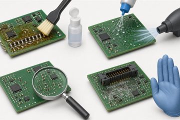
How to Clean a PCB After Soldering: Flux Removal, Drying and Inspection
Learn how to clean a PCB after soldering: identify flux residue, choose a compatible method, avoid re-depositing contamination, dry safely, and inspect the board.



Learn how to clean a PCB after soldering: identify flux residue, choose a compatible method, avoid re-depositing contamination, dry safely, and inspect the board.
A component does not simply release heat into open air. Heat must travel from the semiconductor junction or resistive element through the package, solder connection, PCB copper, vias, thermal interface, enclosure, heat sink, or surrounding air. PCB layout determines how continuous—or restrictive—that path becomes. Two boards using the same component Read more
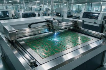
Most articles about laser direct imaging, or LDI, start with the same promise: “LDI improves PCB accuracy, productivity, and yield.” That is not wrong. It is just incomplete. LDI does not magically fix every PCB manufacturing problem. It cannot compensate for poor copper preparation, unstable dry film, incorrect focus, weak Read more
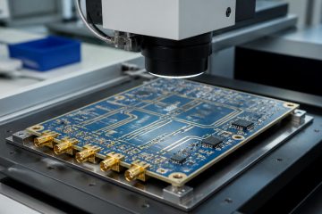
Designing a high frequency PCB is not the same as laying out a standard digital board. Once signals rise above a few hundred MHz, every physical dimension on the board — trace width, dielectric thickness, via geometry, reference plane continuity — starts to affect electrical performance in ways that a Read more
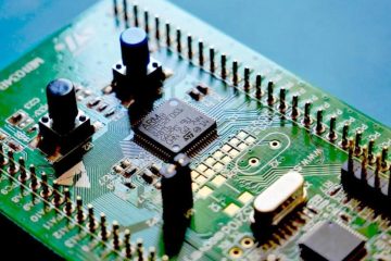
What You Actually Need to Know Before Starting A printed circuit board is a layered structure. At its simplest, you’re looking at three things working together: Most beginner projects use a two-layer board — copper on top, copper on the bottom, connected through drilled and plated holes called vias. That configuration covers the Read more
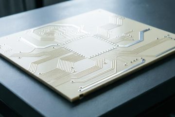
The Material Behind the Magic of Modern Wireless Every generation of wireless technology pushes frequencies higher, data rates faster, and tolerances tighter. The 5G New Radio bands above 24 GHz. Automotive radar operating at 77 GHz. Satellite links bouncing signals across vacuum and atmosphere simultaneously. In each of these domains, Read more
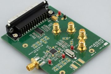
When RF engineers talk about “high frequency PCB,” they’re usually talking about boards that carry signals above 500 MHz — often well into the tens of gigahertz. At those frequencies, every design choice matters: the laminate, the copper surface roughness, the via placement, even the solder mask formulation. A board Read more
Every electronics project starts with a decision most people rush past — picking the wrong board. You’d be surprised how many prototypes end up in the graveyard not because the circuit design failed, but because the substrate underneath couldn’t keep up. After two decades of working with everyone from garage Read more
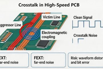
I once worked on a 10 Gbps backboard design that passed every simulation with comfortable margin. Signal integrity looked great. Impedance was controlled. Return loss was within spec. Then the prototype came back, and the eye diagram was a mess. The signals that were supposed to be clean and open Read more
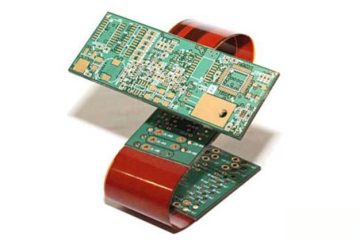
I remember the first time I held a rigid-flex PCB in my hands. It was about twelve years ago, and I was working on a compact sensor module for a medical client. The engineer on the other end of the phone kept insisting that no single rigid board could fit Read more
If you have any enquiry about quotation or cooperation, please feel free to email us at [email protected] or use the following enquiry form. Oursales representative will contact you within 24 hours. Thank you for your interest in our products.