




PCBs are made by turning design data into copper patterns, insulating layers, plated holes, solder mask, surface finish and final tested boards. A factory usually starts with Gerber or ODB++ data review, prepares the copper-clad laminate, images the circuit pattern, etches unwanted copper, drills and plates holes, applies solder mask and silkscreen, finishes the exposed pads, routes the outline and performs electrical testing.
The exact process changes with layer count, copper thickness, minimum trace and spacing, material, via type, impedance control, surface finish and inspection requirements. Understanding the manufacturing flow helps engineers and buyers send clearer files, avoid DFM problems and compare PCB quotations more accurately.
What does it mean to make a PCB?
Making a PCB means fabricating a physical board that connects electronic components through designed copper conductors. The finished bare board normally includes copper traces, pads, vias, laminate material, solder mask, silkscreen markings and a surface finish for solderability.
A PCB is not made from a drawing alone. The factory needs manufacturing files that describe every copper layer, drill, slot, board outline, solder mask opening and printed marking. For a buyer preparing a new order, this is why PCB Gerber files and correct fabrication notes matter before production begins.
What files does a PCB factory need before production?
The factory reviews the file package before releasing the job to production. Missing or unclear data can delay the order or cause the factory to guess details that should be controlled by the designer.
| File or Requirement | Why It Matters | Buyer Check |
|---|---|---|
| Gerber or ODB++ files | Defines copper, solder mask and silkscreen layers | Confirm revision and layer count |
| NC drill file | Defines plated and non-plated holes | Check drill units and hole types |
| Board outline | Controls final shape, slots and cutouts | Make sure there is only one outline |
| Stackup notes | Controls layer order, dielectric and impedance | Required for multilayer or impedance boards |
| Fabrication drawing | States thickness, copper, finish and tolerances | Use it for special requirements |
If the board will later be assembled, keep the bare PCB files aligned with BOM, CPL and assembly drawings. A mismatch between board revision and assembly data can create avoidable PCBA defects.
How are PCB layers prepared before etching?
For a simple two-layer PCB, production begins with copper-clad laminate. For a multilayer PCB, inner copper layers are imaged and etched first, then laminated together with prepreg and outer copper foil under heat and pressure.
Layer preparation is where stackup decisions become real manufacturing constraints. Material type, core thickness, prepreg thickness, copper weight and layer order affect impedance, warpage, drilling, plating and cost. If a design uses high-speed signals, controlled impedance or unusual thickness, review the stackup with the manufacturer before finalizing trace widths.
How are copper traces formed on a PCB?
Copper traces are formed by imaging the circuit pattern and removing unwanted copper. The factory applies a photoresist, exposes it with the PCB artwork, develops the image and chemically etches away copper that is not protected by the pattern.
The practical limit is not only whether a trace can be drawn in CAD. Minimum trace width, spacing, copper thickness and panel process control decide whether the design can be manufactured consistently. This is why a DFM check is useful before releasing boards with fine traces, tight spacing or dense components.
How are PCB holes drilled, plated and inspected?
After layer preparation, the factory drills holes for vias, component leads, mounting screws and tooling features. Mechanical drilling is common for standard holes, while laser drilling may be used for microvias in HDI boards.
Plated through holes need copper deposited on the hole walls so signals can pass between layers. Poor hole quality can cause opens, intermittent failures, assembly problems or reliability issues. Buyers should pay attention to small drill size, aspect ratio, annular ring, via type and copper thickness when a board has dense routing or high current.
What happens after the copper circuit is finished?
After the copper circuit is formed and plated, the factory applies solder mask to protect copper areas that should not be soldered. Openings remain on pads, test points and other exposed copper features. Silkscreen is then printed to show reference designators, polarity marks, logos or handling information.
The exposed pads receive a surface finish such as HASL, lead-free HASL, ENIG, immersion silver, immersion tin, OSP or hard gold. Surface finish affects solderability, shelf life, flatness, cost and application fit. For fine-pitch assembly or wire bonding, the finish choice should be reviewed before ordering.
PCB manufacturing steps checklist
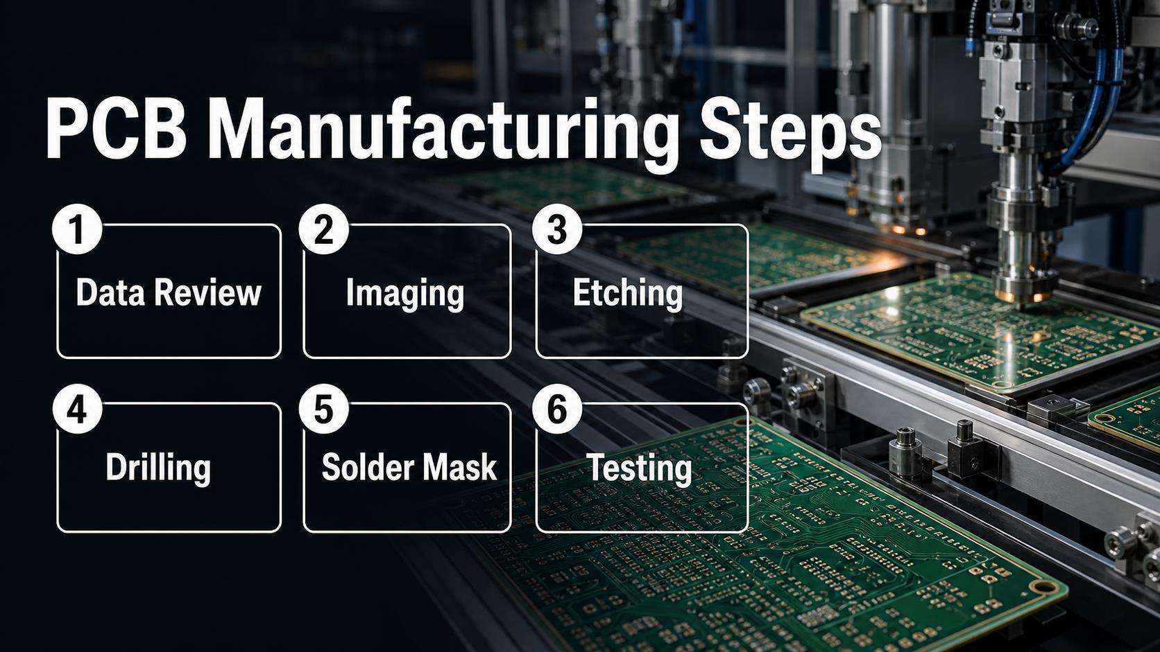
| Step | Factory Action | Buyer Should Confirm |
|---|---|---|
| Data review | Check Gerber, drill and outline data | Correct revision and missing files |
| Imaging | Transfer circuit patterns to copper | Minimum trace and spacing are realistic |
| Etching | Remove unwanted copper | Copper weight matches current and price |
| Drilling | Create vias and holes | Hole size, tolerance and plating notes |
| Solder mask | Protect copper and expose pads | Mask clearance around fine-pitch pads |
| Testing | Check opens, shorts and appearance | Electrical test and special inspection needs |
What PCB specifications change the manufacturing process?
The same PCB outline can have very different manufacturing requirements depending on its specifications. A low-density two-layer board can be straightforward, while a dense multilayer board may require impedance control, tighter registration, smaller drills, higher inspection effort and more careful lamination.
- Layer count: more layers add lamination, registration and stackup control.
- Material: FR-4, high-frequency, aluminum, ceramic and flexible materials use different controls.
- Copper thickness: heavier copper changes etching, spacing and cost.
- Minimum trace and spacing: tighter geometry increases process difficulty.
- Drill size: small holes and high aspect ratio holes need stronger process control.
- Surface finish: ENIG, HASL, OSP and hard gold have different costs and applications.
- Controlled impedance: stackup, trace geometry and material properties must be coordinated.
For manufacturability topics such as spacing, copper balance, annular rings and assembly access, a focused DFM and DFA review can prevent avoidable production questions.
How are finished PCBs tested before shipment?
Finished bare PCBs are normally inspected visually and electrically before shipment. Electrical testing checks whether required nets are connected and whether separate nets are accidentally shorted. Automated optical inspection, final visual inspection, dimensional checks and special tests may also be used depending on the board.
Electrical test does not prove that the final electronic product will work. It confirms the bare board matches the expected connectivity. Functional testing belongs to PCBA or system-level validation after components are assembled.
When should you ask for DFM review before making PCBs?
Ask for DFM review before production when the board has fine-pitch components, small vias, impedance requirements, heavy copper, special materials, unusual thickness, tight tolerances, large panels, slots, controlled bend areas or high reliability requirements.
PCBTRY can review Gerber files, drill data, stackup notes, material requirements, copper weight, surface finish, impedance needs and quantity before fabrication. For a manufacturing review and quote, send your files and requirements to [email protected].
FAQs about how PCBs are made
Are PCBs printed or etched?
PCBs are not printed like paper. The circuit image is transferred to copper, and unwanted copper is etched away. Solder mask and silkscreen are later added as protective and marking layers.
What material are most PCBs made from?
Many standard rigid PCBs use FR-4 laminate with copper foil. Special boards may use high-frequency materials, aluminum, ceramic, polyimide or other substrates depending on heat, frequency, flexibility or reliability needs.
How long does it take to make a PCB?
Lead time depends on layer count, material, process difficulty, quantity, testing and factory workload. Standard prototypes are usually faster than HDI, rigid-flex, heavy copper or controlled-impedance boards.
Why do PCB factories ask questions after Gerber review?
Factories ask questions when data is missing, inconsistent or risky. Common issues include unclear board outline, missing drill file, conflicting layer names, tight spacing, unusual copper weight or missing stackup notes.
Can a PCB be made without Gerber files?
Some manufacturers can use ODB++, IPC-2581 or original CAD exports, but Gerber plus drill files remain widely accepted. A photo, PDF or schematic alone is not enough for normal fabrication.
What is the difference between PCB fabrication and PCB assembly?
PCB fabrication makes the bare circuit board. PCB assembly mounts and solders components onto that board. A finished PCBA may also need programming, inspection and functional testing.
What step creates the green color on many PCBs?
The green color usually comes from solder mask. Solder mask protects copper and leaves openings where soldering is required. Other solder mask colors are also available.
Why does layer count affect PCB price?
More layers require additional imaging, etching, lamination, registration control, drilling and inspection. Higher layer counts can also require more complex stackup control and longer production time.
Does electrical testing mean the PCB will work in my product?
No. Electrical testing checks bare-board continuity and shorts. Product function depends on the circuit design, components, assembly quality, firmware, power conditions and final system testing.
What should I send for a PCB manufacturing quote?
Send Gerber or ODB++ files, drill files, board thickness, copper weight, material, surface finish, solder mask color, quantity, special tolerances, impedance needs and any inspection or test requirements.


