




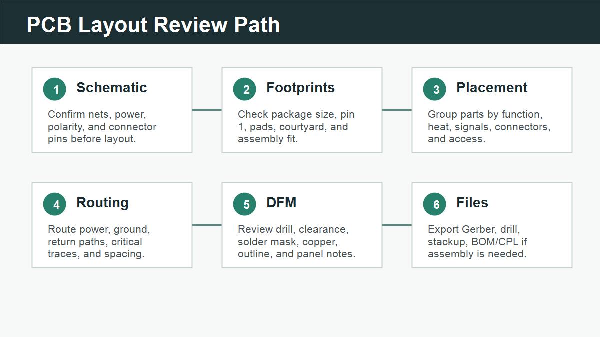
To make a PCB layout, start from a checked schematic, choose verified footprints, place parts by function, route power and ground first, then run electrical and manufacturability checks before exporting Gerber and drill files. A layout is not just a picture of copper traces. It is the point where the circuit, the parts, the board shape, the factory limits, and the future test plan all meet.
This guide shows the layout workflow in a practical order, so a beginner can build a board that is easier to manufacture, inspect, quote, and improve after the first prototype.

Start With a Schematic That Is Ready for Layout
A PCB layout should begin only after the schematic can be reviewed. The schematic must show correct connections, part values, reference designators, connector pin names, power rails, polarity marks, and any special design notes. If the schematic is unclear, the layout may still route successfully but the real board can fail.
Before opening the board editor, check each power input, regulator, MCU, connector, sensor, driver, and protection circuit. If you need a broader starting point, this PCB design basics guide explains how circuit design and board design connect. Ask one simple question: if another engineer looked at this schematic, could they understand what every important net is supposed to do?
Confirm Footprints Before Placing Components
Footprints are where many PCB layout mistakes begin. A footprint must match the real component package, pad size, pin numbering, polarity, height, and assembly clearance. If the footprint is wrong, clean routing cannot save the board.
Check the datasheet land pattern, the supplier package drawing, and the assembly method. For connectors, switches, LEDs, electrolytic capacitors, diodes, and ICs, confirm orientation marks early. A wrong pin 1 marker or reversed connector can turn a good schematic into a bad PCB.
Set Board Shape, Mounting, and Connector Positions First
The board outline should be decided before detailed routing because mechanical limits control where parts can sit. Mounting holes, edge clearance, connector access, enclosure openings, keep-out areas, heat zones, and cable direction all affect the layout.
Place mechanical items first, then lock them. If a connector moves late in the design, nearby traces, ground paths, mounting clearance, and test access may all need to be redone. For production work, include the board outline and any mechanical notes in the files sent for review.
Place Components by Function, Heat, and Signal Flow
Good placement makes routing easier and reduces electrical risk. Group parts that work together: input protection near the connector, regulator parts close to the regulator IC, MCU support parts close to the MCU, and driver circuits close to their loads.
Think of the PCB as paths of current and signal, not as isolated components. High-current, high-speed, switching, analog, RF, and sensor areas should be placed so they do not fight each other. If a sensitive signal must cross a noisy area, the layout should be reconsidered before routing begins.
Route Power, Ground, and Return Paths Before Small Signals
Power and ground decide whether the board behaves reliably. Route high-current paths with enough copper width, short loops, and clear return paths. Ground pours help only when they are continuous and connected correctly; a broken pour can create noise instead of solving it.
For switching regulators, motor drivers, LEDs, relays, and battery paths, review current loops and heat. For boards with higher current or heavier copper needs, the heavy copper PCB design guide gives useful context for copper and heat decisions. For fast digital or RF signals, review the reference plane and return current. The visible trace is only half the route; the return path completes the circuit.
Use Design Rules That Match the Manufacturer
Design rules should reflect real manufacturing capability. Set minimum trace width, spacing, drill size, annular ring, solder mask expansion, copper-to-edge clearance, via size, and preferred tolerances before routing the full board.
| Rule Area | What to Check | Why It Matters |
| Trace width | Current, voltage drop, heat | Prevents overheating and unstable power |
| Clearance | Voltage, fabrication limit, contamination risk | Reduces shorts and arcing risk |
| Drill and via | Minimum drill, annular ring, aspect ratio | Avoids breakout and weak plated holes |
| Solder mask | Mask slivers, pad openings, bridges | Improves assembly yield |
| Board edge | Copper-to-edge and route clearance | Prevents exposed copper and edge damage |
Keep Critical Signals Short, Clear, and Reviewable
Critical signals should be routed with intent. Clocks, USB, RF, impedance-controlled traces, switching nodes, current-sense lines, and sensitive analog inputs should not be treated like ordinary slow control lines.
Keep them short where possible, avoid unnecessary stubs, reduce layer changes, and keep reference paths continuous. If the design has fast edges or controlled-impedance requirements, review these high-speed PCB layout guidelines before freezing the stackup. If the design needs controlled impedance or special material, state that requirement before quotation. Do not assume the manufacturer can guess it from the Gerber files alone.
Add Test Points, Labels, and Debug Access During Layout
Test access is easiest to add while the layout is still flexible. Add points for ground, power rails, programming, reset, communication buses, important analog nodes, and fault signals. A board without test access can be difficult to bring up even when the circuit is correct.
Use readable silkscreen labels when space allows. If the board may go into assembly or production testing, ask the manufacturer what pad size, spacing, and fixture access they prefer before the layout is frozen.
Run ERC, DRC, and DFM Before Exporting Files
ERC checks the schematic logic, DRC checks the layout rules, and DFM checks whether the board can be manufactured reliably. Run all three before sending files for quotation. Each check catches a different kind of problem.
Do not treat a clean DRC as final proof. DRC can miss poor placement, bad return paths, wrong footprints, missing polarity marks, weak test access, or unclear fabrication notes. Use automated checks, then do a human review section by section. For manufacturing-side review, this article on DFM and DFA in PCB manufacturing explains why layout choices affect fabrication and assembly yield.
Prepare Gerber, Drill, Stackup, and Quote Notes
A PCB layout becomes useful to a manufacturer only when the output files are complete. For bare PCB fabrication, prepare Gerber or ODB++ files, NC drill files, board outline, copper weight, thickness, surface finish, solder mask color, quantity, and stackup notes when needed.
If assembly is required, also prepare the BOM, CPL or pick-and-place file, assembly drawing, polarity notes, testing requirements, and approved substitutions. Missing file details can delay quotation or cause avoidable engineering questions.
PCB Layout Checklist Before Manufacturing
Use this checklist before sending a layout for fabrication or assembly review.
- Schematic checked for net names, power rails, polarity, connector pins, and design notes.
- Footprints verified against datasheets and supplier package drawings.
- Board outline, mounting holes, keep-outs, and connectors locked.
- Power and ground paths reviewed for current, heat, and return loops.
- Critical signals reviewed for length, reference path, stubs, and layer changes.
- Design rules matched to manufacturer limits.
- Silkscreen labels, polarity marks, and test points added where useful.
- ERC, DRC, and DFM checks completed.
- Gerber, drill, stackup notes, BOM/CPL if needed, and quote notes prepared.
FAQs About How to Make PCB Layout
What is the first step in making a PCB layout?
Start with a checked schematic. The schematic should show correct nets, part values, power rails, connector pins, polarity, and any special design notes before layout begins.
Can I make a PCB layout without a schematic?
For very simple experimental boards, it may be possible, but it is risky. Most real boards should start from a schematic so nets, components, and future changes can be reviewed.
How do I know if my footprints are correct?
Compare each footprint with the component datasheet and package drawing. Check pad size, pin numbering, polarity, body outline, height, courtyard, and assembly clearance.
Should I place components or route traces first?
Place components first. Good placement creates short, logical routing paths. If placement is poor, routing becomes crowded and electrical risks increase.
What PCB design rules should I set?
Set trace width, spacing, drill size, via size, annular ring, solder mask expansion, copper-to-edge clearance, and any manufacturer-specific limits before routing.
What is DFM in PCB layout?
DFM means design for manufacturability. It checks whether the layout can be fabricated and assembled reliably within the manufacturer’s process limits.
What files are needed after PCB layout?
For fabrication, send Gerber or ODB++ files, NC drill files, board outline, stackup notes, copper weight, finish, quantity, and special requirements. For assembly, also send BOM and CPL files.
Should I add test points to a PCB layout?
Yes, especially for power rails, ground, programming, reset, communication buses, and important debug nodes. Test points help prototype bring-up and production inspection.
Can PCBTRY review my PCB layout before production?
Yes. Send Gerbers, drill files, stackup notes, quantity, surface finish, and BOM/CPL if assembly is needed to [email protected] for DFM and quotation review.
Send PCB Layout Files for DFM Review
If your PCB layout is ready for manufacturing, send Gerber files, NC drill files, board outline, stackup notes, copper weight, surface finish, quantity, and any assembly BOM/CPL files to [email protected]. PCBTRY can review the files for manufacturability, layout risk, file completeness, and quote details before production.



2 Comments
A4988 PCB Layout Guide: Placement, Routing, Grounding and Thermal Checks - thindry pcb manufacturer · 08/25/2026 at 13:03
[…] Keep enough room to route these groups without necking down current paths or cutting the ground plane into accidental islands. This is why a placement plan should precede routing; see PCBtry’s guide to PCB placement, routing, and DFM checks. […]
AI for PCB Layout: What It Can Automate and How to Verify Results - thindry pcb manufacturer · 08/26/2026 at 02:11
[…] An optimizer cannot honor a requirement it cannot see. Before the first run, convert design intent into explicit, reviewable inputs. This is also sound practice for a manual PCB layout workflow. […]