




Start With the EasyEDA PCB Design Workflow
Using EasyEDA for PCB design is not just drawing tracks until the ratlines disappear. A reliable workflow keeps one source of truth from the schematic through footprints, board layout, design-rule checks, Gerber files and NC drill data.
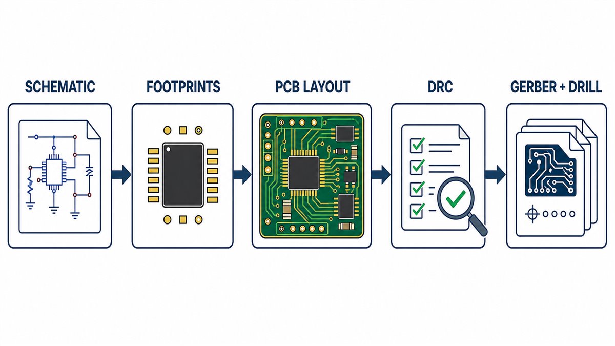
EasyEDA Standard and EasyEDA Pro use different menu names in some places. The engineering sequence is the same: capture the circuit, verify component mapping, convert or update the PCB, define mechanical geometry, place and route, run checks, then inspect the manufacturing package. This guide focuses on that repeatable sequence instead of one editor version’s button positions.
Create the Project and Draw a Readable Schematic
Begin with a project that contains the schematic and PCB under the same design. In EasyEDA Pro this relationship is required for schematic-to-PCB updates; in Standard, keeping the documents together also prevents exporting the wrong revision.
- Create a new project and name the board by product and revision.
- Place symbols from verified libraries or create controlled custom parts.
- Connect nets with wires and meaningful net labels, not visual proximity.
- Add power symbols, connector pin names, polarity and test points.
- Record part numbers and footprint choices before layout begins.
A readable schematic is a test instrument for the design team. Group power entry, regulation, controller, interfaces and loads by function. Someone reviewing the page should be able to follow power and signal flow without tracing a maze of crossing wires.
Verify Symbols, Footprints and Pin-to-Pad Mapping
The symbol tells the schematic what a component does; the footprint tells the PCB where copper pads and holes go. A correct-looking symbol with the wrong footprint can produce a board that cannot be assembled.
| Check | Evidence | Failure if missed |
|---|---|---|
| Pin number to pad number | Datasheet pinout and footprint drawing | Electrically crossed component |
| Package dimensions | Body, pitch, span and exposed-pad dimensions | Part does not fit |
| Polarity and pin 1 | Symbol mark, silkscreen and assembly drawing agree | Reverse assembly |
| Hole and lead size | Finished hole allows lead plus process clearance | Lead cannot be inserted |
| Courtyard and height | Placement clearance and enclosure model | Mechanical collision |
EasyEDA’s official Standard documentation notes that invalid footprint mapping can occur when symbol pin identifiers and footprint pad identifiers differ, including case differences. Do not fix the warning by choosing a package with a similar name. Open the datasheet and verify every mapped pin.
Run Schematic Checks Before Conversion
Before converting to PCB, remove unresolved nets and mapping errors from the source design. Run the available electrical or design checks, then review warnings rather than clearing them as a group.
- Every intended pin is connected or deliberately marked no-connect.
- No two unrelated outputs are tied together.
- Power pins, pull-ups, decoupling capacitors and reset circuits match the component datasheet.
- Connector names describe the external interface and direction.
- Every placed part has an approved footprint and procurement identity.
A schematic check cannot prove the circuit works, but conversion should not begin while the netlist is already known to be inconsistent.
Convert the Schematic to PCB and Manage Updates
In EasyEDA Standard, the official path uses Convert to PCB; later schematic changes can be passed forward with Update PCB or imported from the PCB editor. EasyEDA Pro documents a Schematic to PCB flow and requires the schematic and PCB to belong to the same board.
When conversion stops on footprint errors, return to the footprint manager and correct the source mapping. After conversion, footprints appear with ratlines representing logical nets. Ratlines are not copper tracks; they are reminders of connections that the layout still needs.
For every later schematic revision, update the existing PCB and inspect the proposed change list before accepting it. Confirm added and removed components, renamed nets and footprint changes. Do not create a second PCB file simply to avoid reconciling revisions.
Define the Board Outline, Cutouts and Holes
The board outline is manufacturing geometry, not decoration. Draw one closed, non-overlapping contour on the Board Outline layer. EasyEDA’s documentation warns that an open or overlapping outline is detected during Gerber generation and can also prevent copper pours from displaying correctly.
| Feature | Use | Release check |
|---|---|---|
| Board Outline | Finished external profile | One closed contour with correct dimensions |
| Board cutout / solid region | Internal routed opening | Closed shape, adequate tool radius |
| Hole tool | Non-plated mechanical hole when configured correctly | Finished diameter and plating status |
| Plated pad | Electrical through-hole connection | Pad, drill and annular ring |
Place mounting holes from enclosure datums, not by eye. Add connector overhang, keep-outs and component-height constraints before routing around them.
Set Design Rules From Real Manufacturing Limits
Default design rules are starting values, not proof that a fabricator can build the board economically. Set trace width, clearance, via drill, pad diameter, annular ring, copper-to-edge and mask rules from the selected stackup and supplier capability.
Separate three ideas: the software minimum, the factory’s advertised minimum and your design target. A robust design target normally leaves margin for fabrication tolerance and future volume production. Use tighter values only where the layout truly requires them.
For a deeper release review, compare the design with DFM and DFA checks before generating final files.
Place Components Before Routing
Placement decides most of the routing difficulty. Start with fixed mechanical parts, then arrange components by circuit function and current or signal flow.
- Lock connectors, mounting holes, switches, LEDs and enclosure-critical parts.
- Place power-entry protection and regulators near their source and load paths.
- Put decoupling capacitors next to the correct supply pins with short return paths.
- Keep crystal, feedback and sensitive analog loops compact.
- Check polarity, pin 1, rework access and assembly orientation.
- Leave room for copper pours, test probes and routing channels.
Rotate components to simplify connections, but never rotate away from a clear assembly convention without updating polarity and reference information.
Route Power, Ground and Signals Deliberately
Do not route every net with one default width. Power paths depend on current, copper thickness, allowable temperature rise and voltage drop. Fast or sensitive signals depend on stackup, return path, geometry and separation from noisy nodes.
Route critical loops first, then power, clocks or differential interfaces, ordinary signals and finally low-risk connections. Keep a continuous reference path under signals where the design needs one. Avoid creating plane slots that force return current around a long detour.
Use vias intentionally. Each via changes the current path and consumes annular-ring and clearance space. For high-current or controlled-impedance nets, review via structure with the stackup rather than treating a via as a zero-cost connection.
Add Copper Areas Without Hiding Return-Path Problems
A filled ground area is useful only when it forms a connected, low-impedance return path. After pouring copper, inspect narrow necks, isolated islands, cutouts around pads and traces, and connections between top and bottom ground regions.
Rebuild copper areas after placement or routing changes. Check that thermal reliefs are appropriate for soldering and current, and that high-current pads are not connected through an unintended thin spoke. A visually large pour can still contain a narrow electrical bottleneck.
Run DRC and Resolve Errors Instead of Blindly Ignoring Them
DRC finds geometry that violates configured rules. It does not know whether the rules are correct, whether a footprint matches the purchased part, or whether the circuit will work.
| DRC result | Correct response | Do not do this |
|---|---|---|
| Track-to-pad or net conflict | Check net names and pin-to-pad mapping | Ignore it because copper looks connected |
| Clearance violation | Reroute or document a valid local rule | Reduce the global clearance blindly |
| Trace width violation | Confirm current and purpose of the segment | Assume every neck-down is harmless |
| Unrouted net | Locate the missing connection or correct the schematic | Delete the ratline without evidence |
| Outline error | Close or de-overlap geometry | Hope the manufacturer interprets it |
If an exception is technically justified, record its net, location, reason and reviewer. A clean DRC report achieved by weakening all rules is not a clean design.
Generate Gerber and Drill Files
Generate fabrication outputs only from the approved PCB revision. The manufacturing package normally includes copper layers, solder mask, silkscreen, board outline or mechanical data, NC drill files and fabrication notes.
Keep plated and non-plated drilling intent unambiguous. If the design uses slots, cutouts, blind or buried vias, controlled depth, impedance or special via filling, add explicit notes and confirm the supplier’s preferred data format.
For the role of each layer, see this guide to PCB Gerber files.
Inspect the Manufacturing Package Independently
Do not approve files merely because EasyEDA generated a ZIP. Open the Gerbers and drill data in an independent viewer and inspect the manufactured image, not the editable PCB canvas.
- All expected copper, mask, silkscreen and outline layers are present.
- The board dimensions, cutouts, slots and holes are correct.
- Drill hits align with pads and plated/non-plated intent is clear.
- Polarity marks, pin 1, reference designators and connector labels are readable.
- No copper or mask feature is clipped at the board edge.
- The version in the ZIP matches the approved schematic, BOM and assembly drawing.
This inspection catches wrong-layer, stale-revision and missing-drill failures that a PCB-editor DRC cannot see.
Send the EasyEDA Design for DFM Review
For fabrication review, send the Gerber ZIP, NC drill files, stackup or layer count, finished thickness, copper weight, material, surface finish, minimum feature notes, board quantity and any impedance or special-via requirement. For assembly, also send the BOM, centroid/CPL file, assembly drawings, polarity notes and test requirements.
Contact PCBTRY with this package and request a DFM review before production. The useful request is specific: ask the engineer to check footprint-to-drill fit, annular rings, copper-to-edge clearance, mask openings, fine-pitch assembly risks and whether the files agree with the quotation.
FAQ: EasyEDA PCB Design
Should I use EasyEDA Standard or Pro?
Use the version that supports your project and team, then follow its current official documentation. Menu names differ, but the schematic-to-files engineering flow remains the same.
Can I design a PCB without a schematic?
You can place pads and tracks directly, but you lose a controlled netlist and make DRC conflicts harder to interpret. A schematic-first flow is safer for repeatable manufacturing.
Why will EasyEDA not convert my schematic to PCB?
Common causes include missing footprints, invalid symbol-to-footprint mapping, or pin and pad identifiers that do not match. Correct the source data before conversion.
Does passing DRC mean the PCB will work?
No. DRC checks configured geometry. It does not prove circuit behavior, component selection, footprint accuracy, thermal performance or manufacturability at the chosen supplier.
Why does my copper pour disappear?
An open or invalid board outline can prevent pours from displaying. Also check net assignment, clearance rules and whether the pour needs to be rebuilt.
Are Gerber files enough for PCB assembly?
No. Assembly normally also needs a BOM, centroid/CPL data, assembly drawings, polarity information and test requirements.
Should I ignore a DRC error that looks harmless?
First identify the rule, net, geometry and electrical reason. Use a local documented exception only when the narrower condition is genuinely valid.
What should I check before ordering the first prototype?
Check schematic revision, footprints, outline, holes, DRC, independent Gerber/drill view, BOM availability, assembly orientation and the manufacturer’s DFM feedback.



0 Comments