




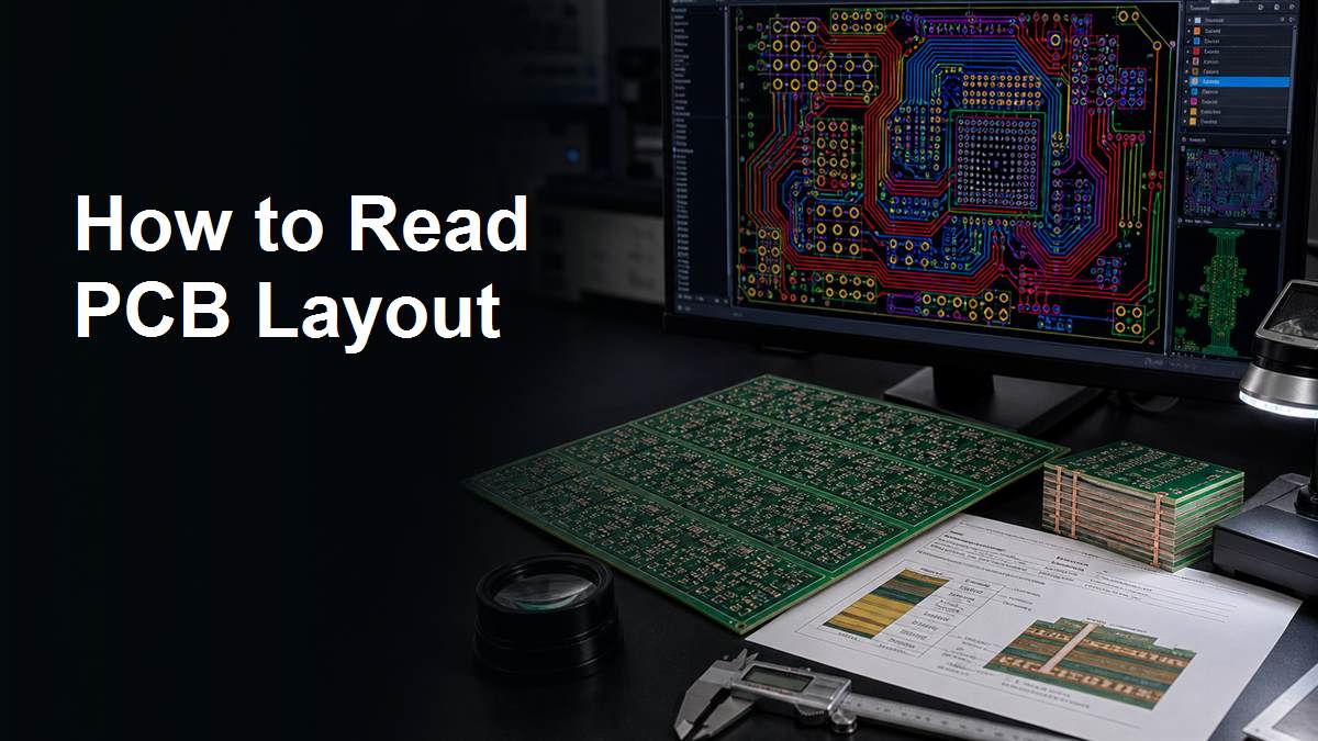
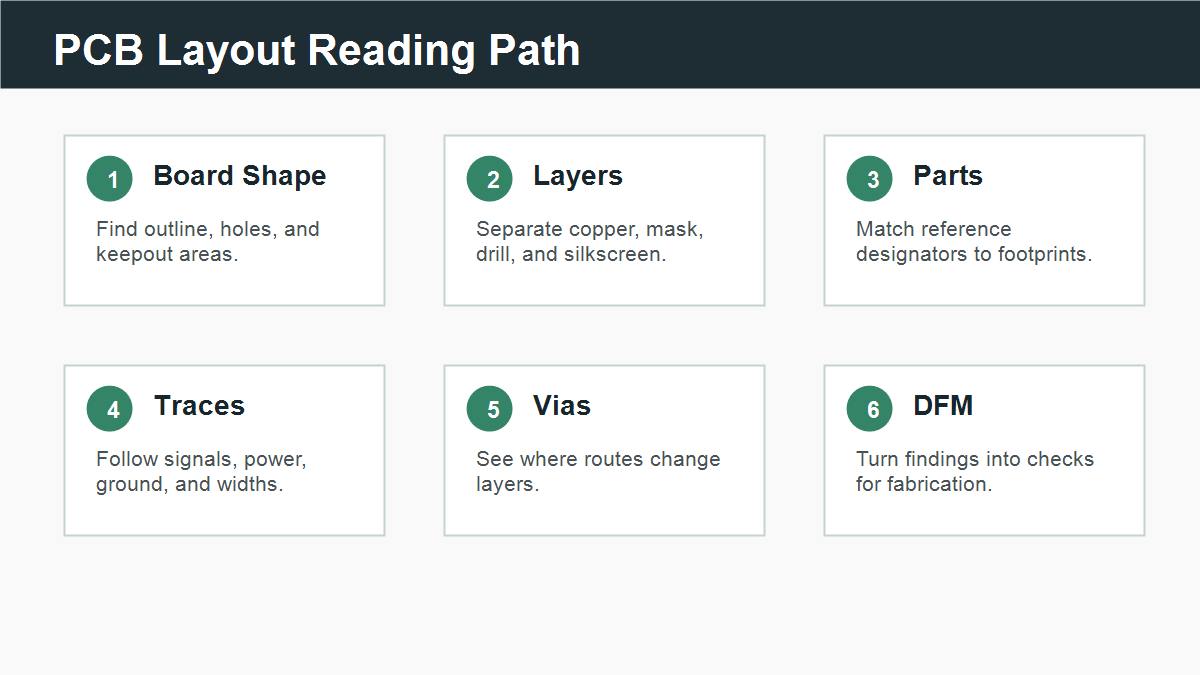
To read a PCB layout, do not start by staring at every line at once. First find the board outline, mounting holes, connectors, layer list, copper layers, drill file, and silkscreen. Then identify components, follow power and ground, trace the important signals, check vias, and finally turn what you see into DFM or quote questions. A PCB layout is a map of how the circuit will become a physical board.
This guide teaches the reading order in plain language, so a beginner can understand what each layout element means and what to check before sending files for fabrication.
Start With the Board Outline and Fixed Parts
The board outline is the physical shape of the PCB. It tells you where the board edge, slots, cutouts, mounting holes, and connector locations are. Read this first because every trace, component, and via must fit inside this physical space.
For example, if a connector must face an enclosure opening, its position matters before you review the routing. A layout that is electrically correct can still fail if the connector, mounting hole, or keepout area is wrong.
Separate Copper, Solder Mask, Silkscreen, and Drill Layers
A common beginner mistake is treating every visible mark as copper. In a Gerber viewer, copper layers show electrical connections. Solder mask layers show where solder mask is opened. Silkscreen shows printed labels. Drill files show holes. These layers answer different questions.
Step 1: turn on only the board outline. Step 2: add top copper and bottom copper. Step 3: add drill holes. Step 4: add solder mask and silkscreen only after the electrical structure is clear.
Match Components to Reference Designators
Reference designators are labels such as R1, C3, U2, D5, or J1. They connect the layout to the BOM and schematic. When you read a layout, match each important footprint to its reference designator and package.
If U1 is a microcontroller, ask where its power pins, reset pin, clock, programming header, and nearby capacitors are. If J1 is a connector, ask which signals enter or leave the board. This turns a visual layout into a functional map.
Follow Power and Ground Before Small Signals
Power and ground are the backbone of the layout. Find the input connector, fuse, regulator, power planes, decoupling capacitors, and ground return path before studying small signal traces. If power is poorly planned, many signals will behave badly even if they are routed neatly.
A simple teaching trick is to ask: where does power enter, where is it converted, where does it go, and how does current return? If you cannot answer that from the layout, the design needs closer review.
Read Traces by Function, Width, and Clearance
A trace is not just a line. Its width, spacing, layer, length, and nearby copper can affect current, impedance, noise, heat, and manufacturability. Wide traces may carry power. Paired traces may be differential signals. Short traces near IC pins may be decoupling or clock-related.
For controlled signals, read this together with PCBTRY’s guide on how to measure PCB trace impedance. The layout view alone is not enough; stackup and target impedance also matter.
Understand Vias as Layer Changes
A via is a plated hole that lets a signal or power net move between layers. When a trace disappears into a via, it usually continues on another copper layer. Beginners often lose the signal at this point, so turn layers on and off to follow it.
For deeper via basics, review PCBTRY’s article on how to make vias on PCB. If a layout uses blind vias, buried vias, or via-in-pad, it may need more advanced manufacturing review.
Use a Table to Read Common Layout Elements
| Element | What It Means | What to Check |
| Outline | Physical board shape | Size, cutouts, mounting holes |
| Pad | Component solder area | Package fit, spacing, polarity |
| Trace | Copper connection | Width, clearance, route path |
| Via | Layer transition | Hole size, annular ring, type |
| Silkscreen | Printed label | Readable, not on pads |
| Drill file | Hole locations | Plated vs non-plated holes |
Turn Layout Reading Into DFM Questions
After you understand the layout, convert observations into manufacturing checks. Ask whether minimum trace width, spacing, drill size, annular ring, solder mask bridge, board thickness, copper weight, and surface finish match the factory capability.
PCBTRY’s DFM and DFA in PCB manufacturing guide is useful here because layout reading should lead to a buildable board, not just a pretty screen view.
PCB Layout Reading Checklist
- Open the files in a Gerber or PCB viewer.
- Check board outline, cutouts, mounting holes, and keepouts first.
- Separate copper, solder mask, silkscreen, and drill layers.
- Match reference designators with BOM and footprints.
- Follow power input, regulators, ground, and return paths.
- Trace important signals and layer changes through vias.
- Check trace width, clearance, drill size, annular ring, and solder mask openings.
- Write down DFM or quote questions before sending the files.
FAQs About Reading PCB Layout
Is a PCB layout the same as a schematic?
No. The schematic shows the electrical idea. The PCB layout shows the physical board, traces, pads, vias, and layers.
What should I look at first in a PCB layout?
Start with the board outline, fixed connectors, mounting holes, and layer list before reading small traces.
What does silkscreen mean on a PCB layout?
Silkscreen is printed text or markings. It helps identify parts, but it is not copper and does not carry current.
How do I follow a trace through a via?
Turn layers on and off in the viewer. The via connects the trace to another copper layer.
Can I read PCB layout without the schematic?
You can understand physical structure, but the schematic helps you know what each net is supposed to do.
What files are needed to review PCB layout for manufacturing?
Send Gerbers, drill files, BOM if assembly is involved, stackup, board thickness, copper weight, and special notes.
What is the biggest beginner mistake?
Reading silkscreen, solder mask, and copper as if they were the same thing. Always separate layers first.
Can PCBTRY review my PCB layout?
Yes. Send Gerbers, drill files, stackup, board thickness, copper weight, quantity, and special requirements to [email protected].
When should I ask for DFM review?
Before fabrication, especially when the layout uses small spacing, small vias, controlled impedance, dense routing, or unusual board shapes.
Send PCB Layout Files for Manufacturing Review
If you need help reading whether a PCB layout is ready for fabrication, send Gerbers, drill files, stackup, board thickness, copper weight, surface finish, quantity, and special requirements to [email protected]. PCBTRY can review manufacturability before production.



0 Comments