




The PCB routing process uses a CNC spindle and a small cutting tool to machine a finished board outline, slots, cutouts and panel separation features. It is selected when a PCB has curves, notches, mixed edge geometry or a smooth profile that V-scoring cannot produce. The routing drawing is therefore a functional manufacturing document: it controls fit, copper-to-edge clearance, tab locations and the stress applied during depaneling.
For engineering review and quotation, send Gerber or ODB++ data, NC drill/rout files, a dimensioned fabrication drawing, finished board thickness, outline tolerances, panel requirements and any keep-out areas near components. PCBTRY can review the profile, panel retention and inspection plan before fabrication so ambiguities are resolved before the router program is released.
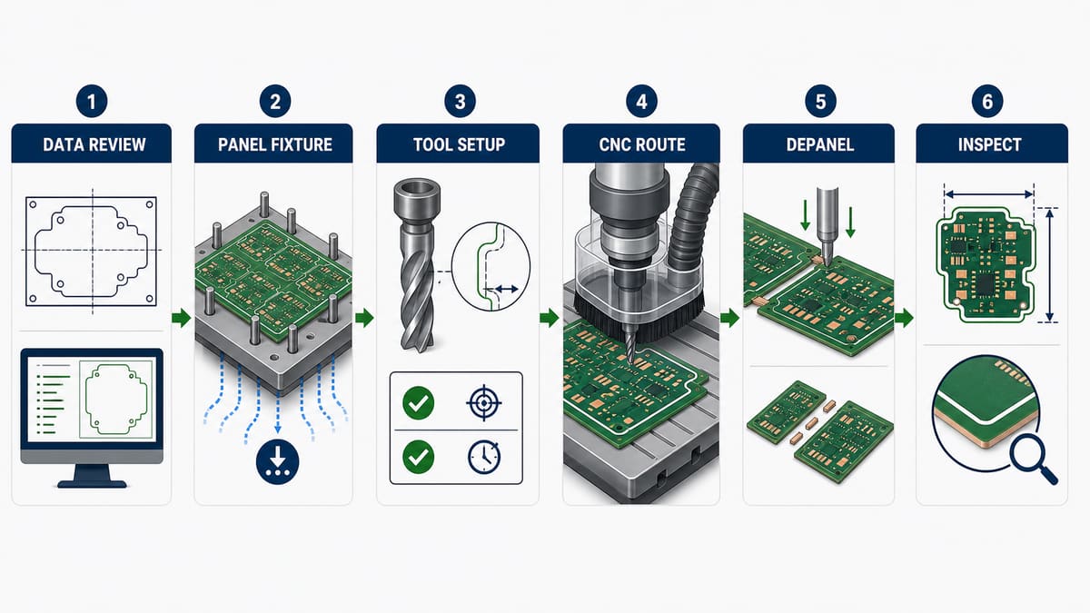
What Is the PCB Routing Process?
PCB routing is a subtractive profile-machining operation, not the electrical trace-routing task performed in PCB design software. A rotating carbide tool follows an NC path around or through the laminated board. The tool has a real diameter, wear condition and direction of cut, so CAM must compensate the path to place the finished edge on the drawing line.
Routing can produce irregular external contours, rounded corners, internal openings and routed slots. It may leave boards loose, retain them in a fabrication panel with tabs, or remove solid tabs after assembly with a controlled depaneling router.
How Does the PCB Routing Process Work?
The factory treats routing as a linked process. A correct NC path cannot recover a wrong outline, and accurate inspection cannot repair a board that moved during cutting.
1. Engineering review and profile reconciliation. CAM compares the Gerber outline, mechanical layer, NC route data and fabrication drawing. Closed contours, slot plating status, radii, datum dimensions and tolerances must agree. Conflicting outlines can produce a board that is internally correct but will not fit its enclosure.
2. Panel and retention planning. The engineer decides how the board will remain stable while material is removed. Tooling rails, support points, vacuum zones and tabs must resist movement without placing break points beside edge connectors, fragile components or thin necks. Too little retention permits chatter or shifting; too much creates difficult, stressful depaneling.
3. Tool and offset setup. Tool diameter, flute condition, spindle behavior, feed and depth strategy are matched to board material and thickness. CAM applies the correct inside or outside offset. A wrong offset changes the finished dimension by a predictable amount, while progressive wear often appears as rougher glass fibers, heat marks or dimensional drift.
4. Fixture registration. The panel is loaded against verified tooling features and supported so it remains flat. The operator confirms program revision, origin and orientation before cutting. A datum mismatch can mirror the intended path or displace every feature even when the machine repeats perfectly.
5. CNC profile routing. The guarded spindle follows the programmed path while local extraction captures FR-4 dust and chips. Entry points, corners and narrow webs deserve special attention because the cutting load changes there. Poor evacuation increases heat and accelerates tool wear; unstable cutting can leave burrs, delamination or a tapered edge.
6. Routed-slot and internal-cutout control. Internal geometry is machined before the external profile when needed to preserve support. Designers must remember that an internal corner cannot be sharper than the effective tool radius unless another approved method is used. Unspecified sharp corners create a fit dispute rather than a machining solution.
7. Depaneling and tab finishing. Boards retained by tabs are separated with the agreed tool or controlled router. The method must support the assembly and limit bending. Manual snapping near ceramic capacitors, BGAs, connectors or thin board sections can transfer strain into solder joints and laminate.
8. Inspection and release. The factory checks the profile against drawing datums, gauges critical dimensions and visually examines edges for burrs, exposed copper, fiber pullout, scorching and delamination. First-article measurements verify the program; sampling or full inspection then follows the documented risk and acceptance plan.
What Data Must Define a Routed PCB Outline?
| Input | What it controls | Risk if unclear |
|---|---|---|
| Closed profile layer | External contour and cutouts | Open, duplicated or competing paths |
| Dimensioned drawing | Datums, critical sizes and tolerances | Nominal geometry without acceptance criteria |
| NC rout/drill data | Machine-readable slots and paths | Plated/non-plated or tool ambiguity |
| Stackup and thickness | Cutting load, support and depth strategy | Burrs, incomplete cut or excessive wear |
| Panel/depanel requirement | Rails, tabs, mouse bites and separation method | Assembly stress or unstable panels |
| Edge keep-outs | Copper, components and connector clearance | Exposed copper or damaged parts |
Use one authoritative profile and state which file governs if data disagree. For the preceding hole operation and its relationship to NC data, see our plated-through-hole process guide.
How Do Toolpaths and Fixtures Affect Edge Quality?
Edge quality is not set by the router bit alone. The result reflects tool offset, wear, cutting direction, entry strategy, panel stiffness, spindle runout and dust removal. If the panel vibrates, the edge can become wavy even with a new tool. If compensation is wrong, the edge may look clean but fail the enclosure dimension.
| Observed result | Likely control to investigate | Buyer evidence |
|---|---|---|
| Rough fibers or heavy burr | Tool wear, feed, support or chip evacuation | First-piece edge photo and tool-life control |
| Dimension consistently oversize/undersize | Tool diameter compensation or wrong contour side | Datum-based measurement report |
| Local notch or entry mark | Lead-in position and path sequence | Approved route program and first article |
| Delamination at a corner | Cutting load, laminate support or worn tool | Magnified edge inspection |
| Tab remnant protrudes | Tab location and finishing method | Post-depanel outline check |
When Should You Choose Routing Instead of V-Scoring?
Choose routing when the finished board needs curves, internal openings, isolated notches or a fully machined edge. V-scoring is usually more efficient for straight-line rectangular arrays, but it imposes geometry and component-clearance constraints and leaves a scored break edge. A hybrid panel can be useful, yet it adds datum and process interactions that should be agreed during DFM rather than added by assumption.
The decision should consider the assembled product as well as the bare board. Route-and-retain panels can support irregular shapes through assembly, while post-assembly router depaneling can reduce bending compared with hand breaking. The right choice is the one that meets outline, component-stress, throughput and handling requirements together.
What Are the Main PCB Routing Failure Modes?
- Wrong profile revision: the route file and fabrication drawing came from different releases.
- Incorrect offset: CAM followed the centerline or compensated on the wrong side.
- Board movement: retention or fixture support was lost before the contour finished.
- Tool wear: edge quality and size drifted after the approved first article.
- Insufficient keep-out: routing exposed copper or contacted an overhanging component.
- Stressful depaneling: a good routed panel was damaged during uncontrolled tab breaking.
These risks should be considered together with material behavior. Our FR-4 substrate material guide explains why the glass-resin laminate needs process-specific handling.
What Tests Verify Routed PCB Quality?
Verification begins with a first article measured from defined drawing datums. Use appropriate optical, mechanical or coordinate measurement for critical external dimensions, slot sizes and location. Visual or magnified inspection then checks edge condition, exposed copper, cracks and laminate separation. A mating gauge or enclosure trial is useful when functional fit matters more than an isolated dimension.
Ask the supplier which dimensions receive first-article, sampling or 100% checks, how tool changes are controlled and how a failed measurement contains the affected quantity. The PCB prototyping process provides a practical way to bind these checks to a build-level verification matrix.
How Do You Choose a PCB Routing Supplier?
Evaluate the supplier’s CAM reconciliation, fixture strategy, tool-life control, extraction, depaneling capability and dimensional inspection—not simply whether a CNC router appears on a capability list. Send the real outline, thickness, panel plan, tolerance, component edge map and enclosure interface. A useful DFM response identifies conflicts and proposes a measurable disposition before production.
- Which file is treated as the authoritative profile?
- How are tool diameter, offset and tool life verified?
- How will the panel remain supported during the final cuts?
- What depaneling method protects edge components and solder joints?
- Which outline features will be measured, and what record is supplied?
Frequently Asked Questions
Is PCB routing the same as electrical trace routing?
No. Manufacturing routing machines the physical board profile. Electrical routing places copper connections in CAD.
Can routing make square internal corners?
A rotating tool leaves a radius related to its diameter. If a true sharp corner is functional, identify it explicitly and ask the manufacturer to review an alternative method or relief geometry.
What files are needed for a routing quotation?
Send Gerber/ODB++, NC data, fabrication drawing, dimensions and tolerances, thickness, panel/depanel requirements and edge keep-outs.
Why are routed board edges rough?
Common causes include tool wear, vibration, unsuitable cutting conditions and poor chip extraction. Inspect both the surface appearance and finished dimensions.
What is tab routing?
The router removes most of the profile but leaves short bridges that retain each board in a panel. Those tabs are later cut or broken using the approved depaneling method.
Does routing damage assembled components?
Controlled routing can limit bending, but poor support, vibration or component interference still creates risk. The fixture and edge keep-out must reflect the assembled board.
How is routing tolerance verified?
Critical features are measured from specified datums with suitable gauges or optical/CMM equipment. Do not rely on the appearance of the edge alone.
Should I specify the router bit diameter?
Specify functional corner radii and dimensions. Let the manufacturer propose a compatible tool unless the tool itself is part of an agreed process requirement.
Request a PCB Routing DFM Review
Send your Gerber or ODB++ package, NC data, drawing, stackup, outline tolerance, panel requirement and component edge map to PCBTRY. We can review profile conflicts, tool access, tabs, depaneling risk and inspection points before providing an engineering evaluation and quotation.



0 Comments