




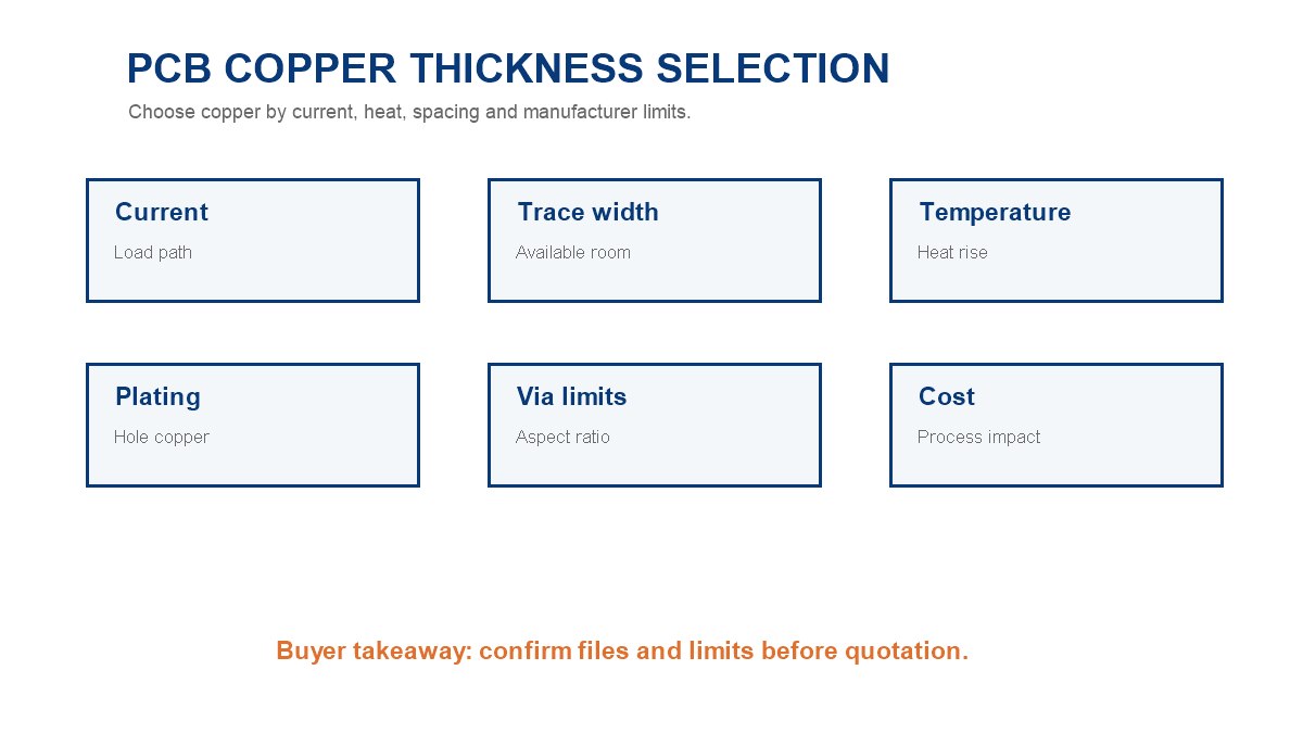
Choose PCB copper thickness by the current the copper must carry, the trace width available, the allowed temperature rise, the layer stackup, via plating needs and manufacturing cost. Do not choose 2 oz or heavy copper just because it sounds stronger. Choose it because the circuit actually needs lower resistance, better heat spreading or higher current capacity.
For most signal boards, common copper can be enough. For power, motor control, LED, charging, industrial control or thermal designs, copper thickness should be confirmed before quotation because it can affect trace spacing, etching, drilling, plating and lead time.
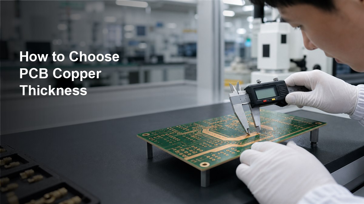
What PCB Copper Thickness Means
PCB copper thickness means the amount of copper used on a PCB layer. It is often described in ounces, such as 1 oz copper or 2 oz copper, but the real decision is about electrical current, heat and manufacturability.
How 1 oz and 2 oz Copper Compare
1 oz copper is common for many standard PCBs. 2 oz copper is thicker and can carry more current when the layout and spacing support it.
| Copper | Typical Use | Buyer Check |
| 0.5 oz | Fine signals or inner layers | Check current and fabrication limits |
| 1 oz | Common signal and moderate power boards | Good default for many projects |
| 2 oz | Higher current or heat spreading | Check spacing, etching and cost |
| 3 oz+ | Heavy copper applications | Requires early factory review |
Start With Current Load and Temperature Rise
The first real question is how much current the trace must carry and how much heat rise the product can tolerate. Higher current needs wider traces, thicker copper or both.
Step 1: Identify the maximum continuous current.
Step 2: Decide the acceptable temperature rise.
Step 3: Check whether the available trace width can support that current.
Step 4: If the trace becomes too wide, consider thicker copper or a different layout.
Check Trace Width Before Increasing Copper
Thicker copper is not a magic fix. If trace spacing is already tight, thicker copper can make etching and clearance more difficult.
A board with enough routing space may solve the current problem with wider traces. A dense board may need a stackup change, copper pour, multiple layers or heavier copper.
Understand Outer Copper and Inner Copper
Outer copper and inner copper may not be the same after manufacturing. Outer layers can gain copper through plating, while inner layers are usually defined before lamination.
When copper is critical, ask whether the quote refers to base copper or finished copper. This is especially important for controlled current paths and plating requirements.
How Via Plating Affects Copper Decisions
Via plating affects how current moves between layers. A thick surface trace still fails the design if the vias cannot carry the current safely.
Use enough vias, suitable drill sizes and practical annular rings. For high current, ask the manufacturer to review via count, via size and plating assumptions.
When Heavy Copper PCB Is the Right Choice
Heavy copper PCB is the right choice when current, heat or durability requirements exceed what ordinary copper can handle comfortably. It is common in power electronics, charging, motor control and industrial equipment.
Before using heavy copper, review the impact on line spacing, solder mask, etching, board thickness and price. See heavy copper PCB design considerations for related limits.
How Copper Thickness Affects PCB Cost
Copper thickness affects cost because thicker copper can require more material, longer processing, wider clearances and stricter inspection. It may also reduce panel yield if the design is dense.
How Stackup and Material Affect Copper Choice
The stackup and material system affect how copper performs. A copper decision should be checked with the laminate, board thickness, layer count and thermal path.
For material background, review copper clad laminate and FR-4 substrate material before finalizing the stackup.
What to Put in the RFQ
The RFQ should state copper thickness clearly for each layer. Do not only write “standard copper” if the current path matters.
- Layer count and stackup.
- Outer and inner copper weight.
- Finished copper or base copper expectation.
- High-current nets or copper pours.
- Via current requirements.
- Surface finish and board thickness.
- Quantity and lead time.
Common Mistakes When Choosing Copper Thickness
The most common mistake is choosing copper by habit instead of by load. Another mistake is increasing copper but forgetting trace spacing, via plating and manufacturer capability.
Also avoid mixing copper thickness with board thickness. If both are critical, connect the copper decision with PCB thickness tolerance and stackup review.
PCB Copper Thickness Selection Checklist
| Check | Question | Action |
| Current | How much current flows? | Calculate trace and via needs |
| Heat | How much rise is acceptable? | Review copper area and airflow |
| Spacing | Can the board be etched reliably? | Check DFM limits |
| Vias | Can layer changes carry current? | Add via count or size |
| Cost | Is thicker copper necessary? | Quote alternatives |
FAQs About PCB Copper Thickness
Is 1 oz copper enough for most PCBs?
For many signal and moderate-load boards, yes. Power and thermal designs need current and temperature checks.
When should I use 2 oz copper?
Use 2 oz when current, heat or voltage drop requires more copper and the layout can support the spacing.
Does thicker copper always improve reliability?
No. It helps only when matched to the design. It can create manufacturing challenges if used unnecessarily.
Does copper thickness affect impedance?
It can affect trace geometry and loss. For high frequency projects, confirm stackup and impedance with the manufacturer.
Does copper thickness affect PCB price?
Yes. Thicker copper can increase material cost, process time and DFM restrictions.
What is finished copper?
Finished copper is the copper thickness after plating and manufacturing, especially relevant on outer layers.
Can I mix different copper weights by layer?
Often yes, but the stackup and manufacturing capability must be reviewed.
What files help confirm copper thickness?
Gerbers, stackup, fabrication notes, current path notes and quantity help the supplier review feasibility.
Should I ask for DFM review?
Yes, especially for 2 oz, 3 oz or heavier copper boards.
Send Copper Thickness Requirements for Review
If you need help choosing PCB copper thickness, send your Gerber files, stackup, current requirements, board thickness and target quantity to [email protected]. PCBTRY can review whether the copper choice fits the current load, heat, spacing and manufacturing limits.



2 Comments
A4988 PCB Layout Guide: Placement, Routing, Grounding and Thermal Checks - thindry pcb manufacturer · 08/26/2026 at 08:31
[…] Document the calculation and ask the fabricator to confirm finished copper assumptions. PCBtry’s copper-thickness review guide explains why nominal copper weight alone does not establish a current […]
PCB Copper Plating Process: Bath Control, Thickness and Quality Checks - thindry pcb manufacturer · 08/29/2026 at 11:02
[…] but they do not remove the need for design limits. For related design decisions, review how to choose PCB copper thickness and how via geometry and plating affect […]